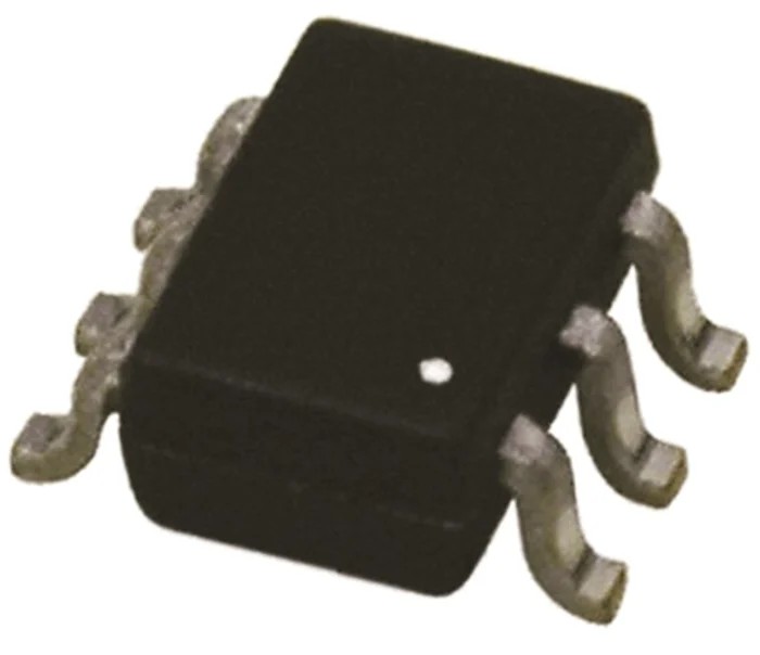
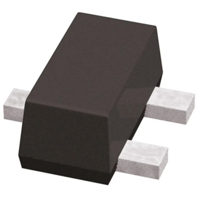
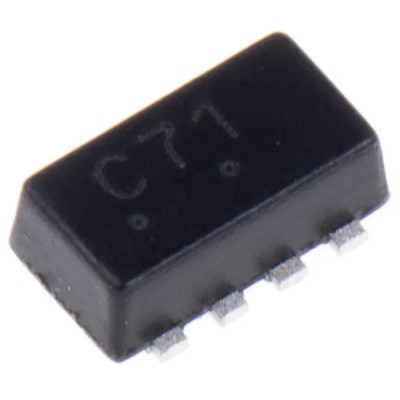
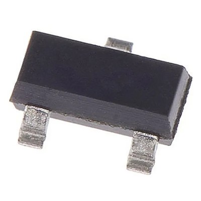
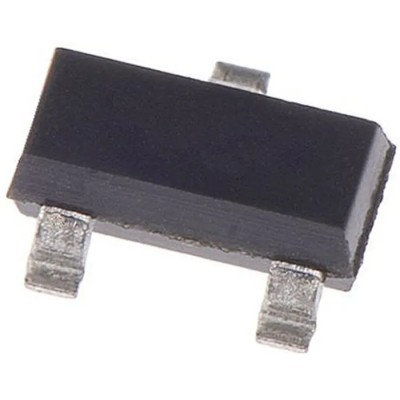
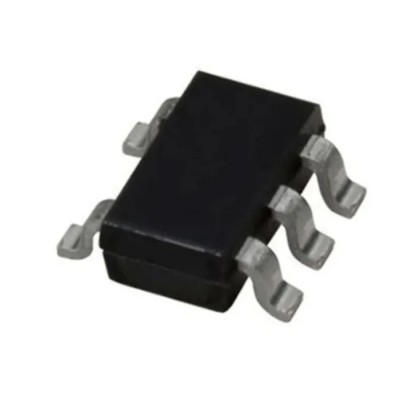
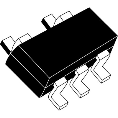
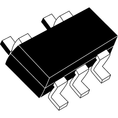
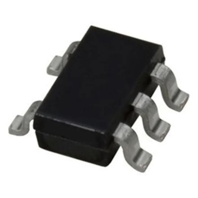
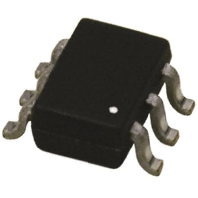
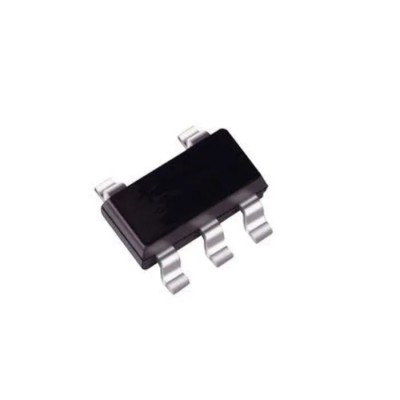
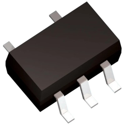
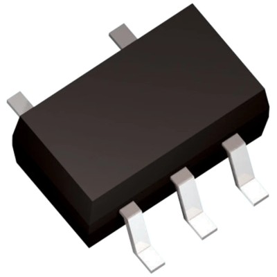
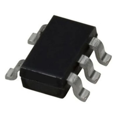
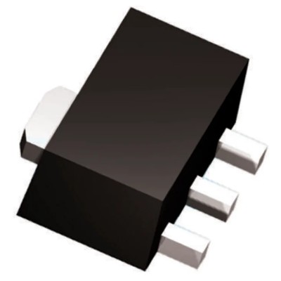
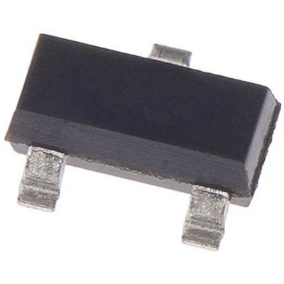
DiodesZetex DMN63D8LDW-7 is an advanced isolated dual N-Channel power MOSFET designed for efficient power switching. With a continuous drain current rating of 260 mA and a maximum drain-source voltage of 30 V, this device offers reliable performance for low power electronic circuit applications. Its compact SC-88 package with 6 pins facilitates integration in miniature and surface-mount designs.
The MOSFET operates in enhancement mode and features a low drain-source resistance (Rds) of 13 Ω, allowing for minimized conduction losses and improved efficiency. The device's maximum power dissipation rating of 400 mW ensures safe energy handling under typical operating conditions. It maintains stable performance in extreme temperature environments ranging from -55°C up to +150°C, making it appropriate for automotive and industrial applications.
With a typical gate charge of only 0.4 nC at Vgs, the MOSFET supports fast switching frequencies, which is crucial for high-speed circuits. Its physical dimensions - length of 2.2 mm, width of 1.35 mm, and height of 1 mm - enable compact PCB layouts where space is limited. The device comprises two elements per chip, enhancing functionality within the small package footprint.
This product complies with multiple industry and safety standards including UL 94V-0 flammability, J-STD-020 for moisture sensitivity, MIL-STD-202 for environmental testing, RoHS for hazardous substance control, and the automotive qualified AEC-Q101 standard, guaranteeing reliability and performance in demanding applications.
Typical use cases include power management in consumer electronics, automotive electronics, industrial controls, and compact power supplies. The isolated dual N-Channel configuration is particularly suited for applications requiring efficient parallel switching or dual switching channels on a single chip.
Choose DiodesZetex DMN63D8LDW-7 to ensure dependable and compliant performance in a small, surface-mount compatible package. This dual N-Channel MOSFET features low drain-source resistance of 13 Ω for efficient power handling.
Maximum power dissipation is rated at 400 mW, suitable for low power switching applications. The device operates across a wide temperature range from -55°C to +150°C ensuring robustness in various environments. Typical gate charge is minimal at 0.4 nC for fast switching capability.
Package dimensions measure approximately 2.2 mm length, 1.35 mm width, and 1 mm height for space-constrained designs. Configured with two elements per chip in an enhancement mode channel configuration. Complies with automotive standard AEC-Q101 and safety standards UL 94V-0, J-STD-020, MIL-STD-202, RoHS for reliability and environmental compliance.
Pin count of 6 enables easy integration onto printed circuit boards with surface mount technology.
Explore more Power MOSFETs and advanced semiconductor components in the Electronics & Electricals category at EnvMart for your industrial, automotive, and electronic design requirements.






Comments (0)
Your review appreciation cannot be sent
Report comment
Report sent
Your report cannot be sent