$1.82
$1.77
Tax included

World's First Climate Tech Platform | Free Delivery in India | Global Shipping

Shop with confidence knowing that our 24/7 Customer Support is always available to assist with any inquiries

Avail maximum benefits from input tax mechanism on all your Business Invoices. Get GST Invoices on your business purchases. And 0% Taxes on all worldwide deliveries

If you find this product anywhere at lower cost than us. Call us and we will not only match the price but also give a complimentary coupon

Shop with assurance, as each product we offer is 100% original, ensuring quality and authenticity with every purchase
| Country of Origin | India |
|---|---|
| Brand | onsemi |
| Height | 4.83mm |
| Length | 10.67mm |
| Model | FQB12P20TM |
| Width | 9.65mm |
| Mount Type | Surface |
| Series | QFET |
| Maximum Operating Temperature | 150°C |
| Package Type | TO-263 |
| Minimum Operating Temperature | -55°C |
| Pin Count | 3 |
| Channel Type | Type P |
| Maximum Continuous Drain Current Id | 11.5A |
| Maximum Drain Source Voltage Vds | 200V |
| Maximum Drain Source Resistance Rds | 470mΩ |
| Channel Mode | Enhancement |
| Maximum Power Dissipation Pd | 3.13W |
| Typical Gate Charge Qg @ Vgs | 31nC |
| Maximum Gate Source Voltage Vgs | -30, +30V |
| Forward Voltage Vf | -5V |
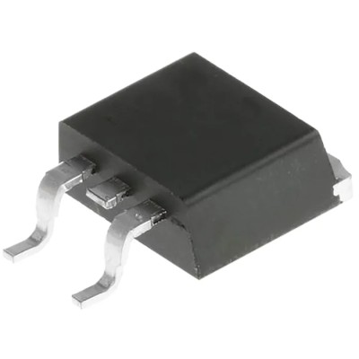
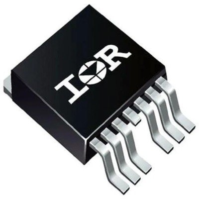
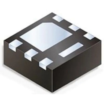
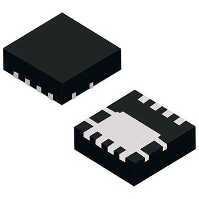
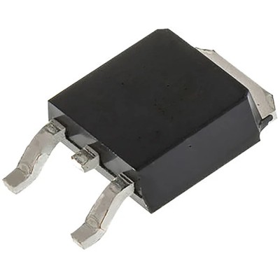
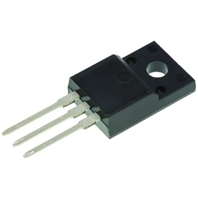
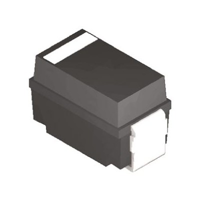
onsemi FQB12P20TM is a QFET Type P-Channel MOSFET designed with enhancement mode operation, capable of handling a continuous drain current of 11.5 amperes and a maximum drain-source voltage of 200 volts. Packaged in a TO-263 surface mount configuration with three pins, this device leverages ON Semiconductor's proprietary high cell density DMOS technology, providing low on-resistance and rugged, reliable switching characteristics.
Its robust electrical ratings include a maximum power dissipation of 3.13 watts and a wide operating temperature range from -55°C to 150°C, making it suitable for demanding industrial and commercial electronic applications.
The MOSFET features a maximum drain-source resistance of 470 milliohms, ensuring efficient conduction and minimal power loss. The typical gate charge of 31 nanoCoulombs allows for fast switching, which is valuable in high-frequency power circuits. It supports gate-source voltages ranging between -30 V and +30 V, providing strong gate protection margins.
Physically compact, the device measures 10.67 mm in length, 9.65 mm in width, and 4.83 mm in height, optimized for space-constrained PCB layouts.
Key applications include load switching, DC/DC converter circuits, battery protection schemes, power management control systems, and DC motor control, underscoring its versatility across industrial, manufacturing, automotive, and consumer electronics sectors.
This P-Channel MOSFET serves as a voltage-controlled switch enabling efficient load switch operations. Manufactured with high-density DMOS technology to reduce on-state resistance and improve reliability. The device delivers high saturation current capability suitable for power management tasks.
Designed for high-speed switching applications with superior ruggedness and durability. Suitable for a wide temperature range from sub-zero to elevated industrial temperatures. Compact 3-pin TO-263 package supports surface mount assembly methods.
Applications span load switching, DC/DC converters, battery protection, and motor control.
Explore the Electronics & Electricals category at EnvMart for a comprehensive range of semiconductors and MOSFET devices from leading brands such as onsemi for your electronic design and production needs.
Review sent
Your review cannot be sent
Global Payments 140+ Countries
Global Shipping Fedex/UPS/DHL/Aramex/
BlueDart/Delhivery/DP World
24/7 Customer Support Email/Chat/Telephonic Support
Comments (0)
Your review appreciation cannot be sent
Report comment
Report sent
Your report cannot be sent