$0.33
$0.32
Tax included

World's First Climate Tech Platform | Free Delivery in India | Global Shipping

Shop with confidence knowing that our 24/7 Customer Support is always available to assist with any inquiries

Avail maximum benefits from input tax mechanism on all your Business Invoices. Get GST Invoices on your business purchases. And 0% Taxes on all worldwide deliveries

If you find this product anywhere at lower cost than us. Call us and we will not only match the price but also give a complimentary coupon

Shop with assurance, as each product we offer is 100% original, ensuring quality and authenticity with every purchase
| Country of Origin | Japan |
|---|---|
| Brand | Toshiba |
| Height | 0.9mm |
| Length | 1.25mm |
| Model | SSM6N35FU(TE85L,F) |
| Width | 1.25mm |
| Mount Type | Surface |
| Series | SSM6 |
| Maximum Operating Temperature | 150°C |
| Package Type | US6 |
| Minimum Operating Temperature | -55°C |
| Pin Count | 6 |
| Number of Elements per Chip | 2 |
| Channel Type | N |
| Maximum Continuous Drain Current Id | 180mA |
| Maximum Drain Source Voltage Vds | 20V |
| Maximum Drain Source Resistance Rds | 20Ω |
| Channel Mode | Enhancement |
| Maximum Power Dissipation Pd | 200mW |
| Maximum Gate Source Voltage Vgs | -10, +10V |
| Forward Voltage Vf | -0.9V |
| Transistor Configuration | Isolated |
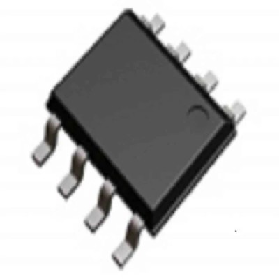
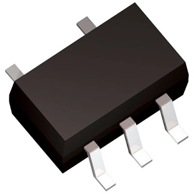
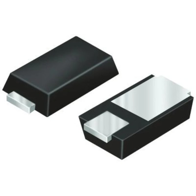
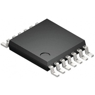
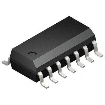
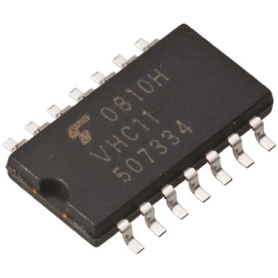
Toshiba SSM6N35FU(TE85L,F) is a dual isolated N-Channel MOSFET transistor designed for discrete semiconductor applications. It supports a maximum continuous drain current of 180mA and can withstand a maximum drain-source voltage of 20V, making it suitable for compact power switching and amplification circuits.
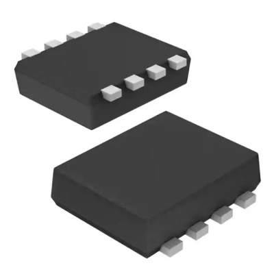
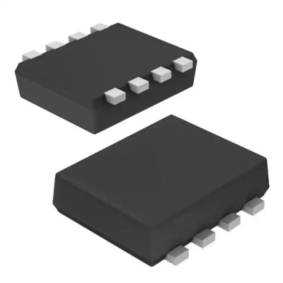
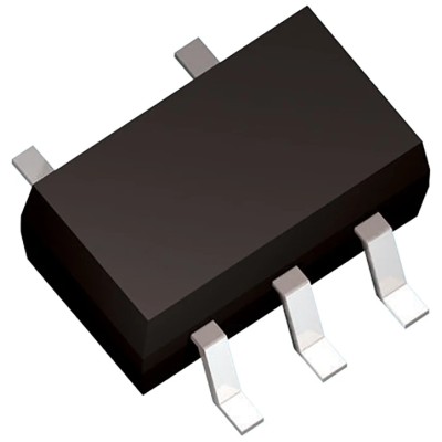
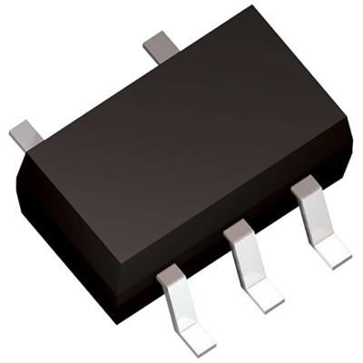
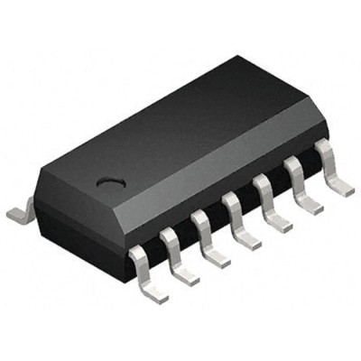
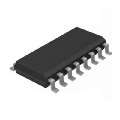
The transistor is housed in a 6-pin US6 surface-mount package, providing a small form factor (1.25mm length x 1.25mm width x 0.9mm height) for easy integration on printed circuit boards. Its enhancement mode operation ensures efficient control of the current flow when a gate voltage is applied.
This component features a maximum power dissipation of 200mW and a drain-source resistance of 20Ω, offering reliable thermal handling capabilities. It operates safely within a temperature range of -55°C to 150°C, suitable for a variety of industrial and commercial electronic environments.
The device also provides a forward voltage of -0.9V and supports a maximum gate-source voltage between -10V and +10V, ideal for precise control in low voltage logic circuits. Each chip contains two elements to accommodate dual switching functions within a compact footprint.
Maximum continuous drain current of 180mA. Rated for 20V drain-source voltage. Surface mount 6-pin US6 package for space-efficient PCB layouts. Enhancement mode with isolated transistor configuration. Max power dissipation of 200mW ensures thermal stability.
Wide operating temperature range from -55°C to 150°C enables durability. Forward voltage drop of -0.9V for efficient conduction. Dual elements per chip increase functional performance.
Commonly used in electronics manufacturing, power management, signal processing, and embedded systems, this Toshiba MOSFET is well-suited for industrial, commercial, and laboratory applications requiring reliable N-channel switching devices. Its compact size and enhanced electrical characteristics help engineers optimize circuit designs for efficiency and durability.
Explore a comprehensive range of semiconductor and discrete electronic components in the MOSFET category at EnvMart for your precise project requirements.
Review sent
Your review cannot be sent
Global Payments 140+ Countries
Global Shipping Fedex/UPS/DHL/Aramex/
BlueDart/Delhivery/DP World
24/7 Customer Support Email/Chat/Telephonic Support
Comments (0)
Your review appreciation cannot be sent
Report comment
Report sent
Your report cannot be sent