Previous
Next
Share
Free Delivery in India | Lowest Global Shipping Charges
24/7 Customer Support

Shop with confidence knowing that our 24/7 Customer Support is always available to assist with any inquiries

24/7 Customer Support
Save up to 28% with GST Input

Avail maximum benefits from input tax mechanism on all your Business Invoices. Get GST Invoices on your business purchases. And 0% Taxes on all worldwide deliveries

Lowest Price Challenge
# Lowest Price Challenge

If you find this product anywhere at lower cost than us. Call us and we will not only match the price but also give a complimentary coupon

Lowest Price Challenge
100% Original Products

Shop with assurance, as each product we offer is 100% original, ensuring quality and authenticity with every purchase

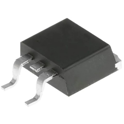
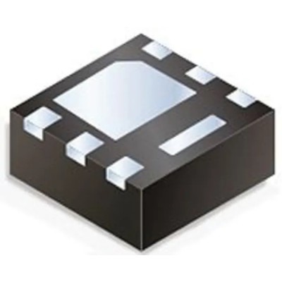
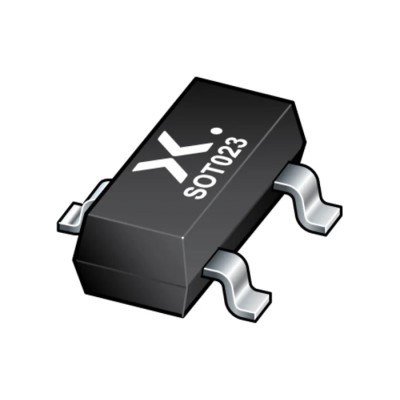
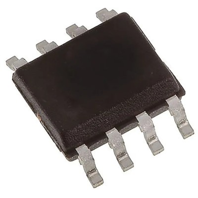
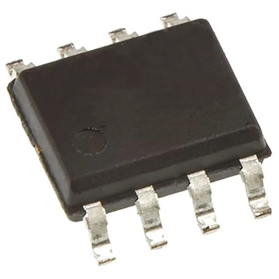
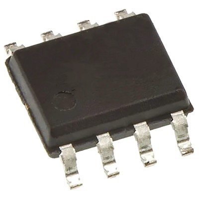
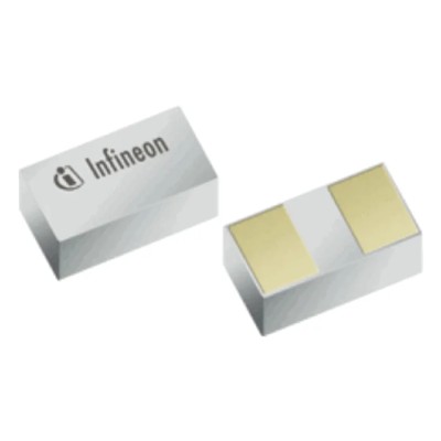
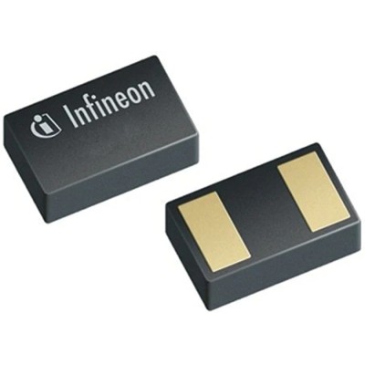
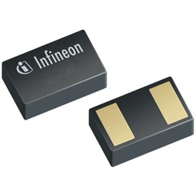
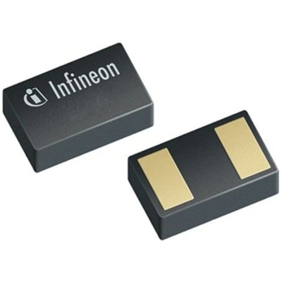
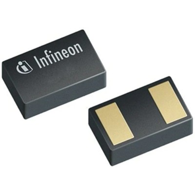
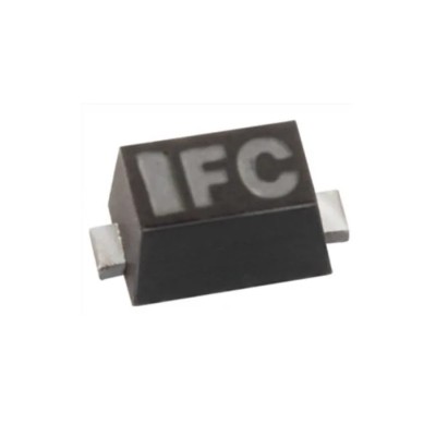
Infineon Dual OptiMOS 1 Type P, Type N-Channel MOSFET Arrays 2.3A 30V Enhancement 6-Pin TSOP BSL308CH6327XTSA1

Category MOSFET Brand Infineon Condition New

Specifications

Country of Origin India
Brand Infineon
Height 1mm
Length 2.9mm
Model BSL308CH6327XTSA1
Width 1.6mm
Mount Type Surface
Series OptiMOS
Maximum Operating Temperature 150°C
Package Type TSOP
Minimum Operating Temperature -55°C
Standards/Approvals IEC61249-2-21, RoHS
Pin Count 6
Number of Elements per Chip 1
Automotive Standard AEC-Q101
Channel Type Type P, Type N
Maximum Continuous Drain Current Id 2.3A
Maximum Drain Source Voltage Vds 30V
Maximum Drain Source Resistance Rds 57mΩ
Channel Mode Enhancement
Maximum Power Dissipation Pd 0.6W
Typical Gate Charge Qg @ Vgs -5nC
Maximum Gate Source Voltage Vgs 20V
Forward Voltage Vf 1.1V
Transistor Configuration Dual

Key Features

  • Maximum continuous drain current of 2.3A enables moderate load handling.
  • Maximum drain-source voltage rating of 30V supports 30V system architectures.
  • Low Rds(on) of 57mΩ reduces conduction losses and heat generation.
  • Rated for operation from -55°C up to 150°C for harsh thermal environments.
  • Dual transistor configuration with one element per chip delivering both P- and N-channel functions.
  • Maximum gate-source voltage of 20V protects gate integrity under transient conditions.
  • Forward voltage of 1.1V improves efficiency in diode conduction paths.
  • AEC-Q101 automotive standard compliant for reliable automotive applications.

Product Description

Infineon BSL308CH6327XTSA1 is a dual OptiMOS MOSFET array combining P-channel and N-channel enhancement mode transistors in a compact 6-pin TSOP surface-mount package. This device is optimized for switching and power management tasks in automotive and industrial electronics with a maximum continuous drain current of 2.3 amperes and maximum drain-source voltage of 30 volts. Its low on-resistance (57mΩ) minimizes conduction losses and heat generation, enabling efficient operation.

Capable of operating over a wide ambient temperature range from -55°C to 150°C, the BSL308CH6327XTSA1 supports robust usage in harsh thermal environments. The device offers a maximum gate-source voltage of 20 volts to protect gate integrity during voltage transients and features a forward voltage of 1.1 volts to improve efficiency in diode conduction paths.

Designed for surface-mount assembly on standard PCB land patterns, its compact dimensions of 2.9mm length, 1.6mm width, and 1mm height make it ideal for high-density circuit designs. The transistor configuration is dual with one element per chip, delivering both P- and N-channel functionality suitable for switching applications in motor driver circuits, DC-DC converters, battery management, and power distribution.

The product complies with RoHS directives and IEC61249-2-21 material standards, ensuring environmentally friendly manufacturing. Additionally, it meets the AEC-Q101 automotive qualification standard, making it suitable for automotive body control modules and other demanding electronics requiring automotive-grade reliability.

Use cases for this MOSFET array include automotive body control modules, high density DC-DC switching stages, battery management systems, and motor driver low-side or high-side switching. The dual transistor design supports compact PCB layouts where space is constrained and component integration is critical.

Package contents include one MOSFET array in a 6-pin TSOP package. This component provides reliable operation and efficient switching performance in industrial, automotive, and commercial electronics applications.

Maximum continuous drain current of 2.3 amperes. Maximum drain-source voltage of 30 volts supports automotive architectures. Low Rds(on) 57 milliohms for efficiency. Operating temperature range from -55°C to 150°C. Dual transistor configuration with P- and N-channel transistors.

Maximum gate-source voltage 20 volts for gate protection. Forward voltage 1.1 volts for diode conduction efficiency. AEC-Q101 automotive standard compliant for quality assurance. Compact TSOP 6-pin surface-mount package.

Explore additional Infineon MOSFET arrays and semiconductor components in EnvMart's Electronics & Electricals category for advanced power management solutions.

Infineon Dual OptiMOS 1 Type P, Type N-Channel MOSFET Arrays 2.3A 30V Enhancement 6-Pin TSOP BSL308CH6327XTSA1
Looking to purchase in bulk?
  • Purchase item in bulk quantity

  • Get best price for your business

Comments (0)

No customer reviews for the moment.

Frequently Asked Questions

The maximum continuous drain current of the BSL308CH6327XTSA1 is 2.3A.

This model has a maximum drain-source voltage rating of 30V, suitable for 30V system architectures.

It is rated for operation from -55°C to 150°C, making it suitable for harsh thermal environments.

The low Rds(on) value is 57mΩ, which helps reduce conduction losses and heat generation.

The maximum gate-source voltage for this MOSFET array is 20V, which protects gate integrity under transient conditions.

The forward voltage is 1.1V, which improves efficiency in diode conduction paths.

This model has a length of 2.9mm, a width of 1.6mm, and a height of 1mm.

It is designed for surface mounting on standard PCB land patterns.

It complies with RoHS directives and IEC61249-2-21 material standards, ensuring environmentally friendly manufacturing.

Yes, it meets the AEC-Q101 automotive qualification standard, making it suitable for automotive body control modules and other demanding applications.

Each chip contains one element, providing both P-channel and N-channel functionality in a dual configuration.

It is suitable for applications such as automotive body control modules, DC-DC converters, battery management systems, and motor driver circuits.

Related Products

Other Products from this brand

$0.35
$0.34 Save 3%
Tax included
Quantity
Delivery Time Delivered within 0-3 days
  • Global Payments 140+ CountriesGlobal Payments 140+ Countries
  • Global Shipping Fedex/UPS/DHL/Aramex/
BlueDart/Delhivery/DP WorldGlobal Shipping Fedex/UPS/DHL/Aramex/ BlueDart/Delhivery/DP World
  • 24/7 Customer Support Email/Chat/Telephonic Support24/7 Customer Support Email/Chat/Telephonic Support
$0.35
$0.34
Tax included