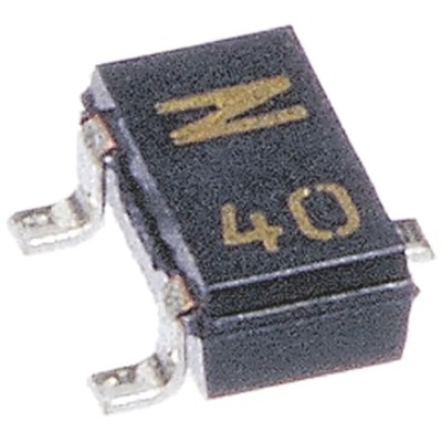
DiodesZetex ZXMN3A01ZTA is a high-quality N-Channel Enhancement mode MOSFET specifically designed for efficient electronic switching applications requiring moderate current capacity and low voltage operation. Rated for a maximum continuous drain current of 3.3 A and a maximum drain-source voltage of 30 V, this MOSFET supports reliable performance in electronic circuit designs including power management, signal amplification, and switching regulators.
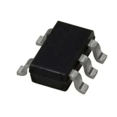
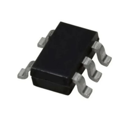
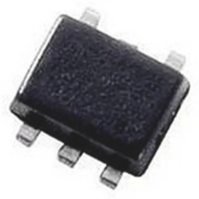
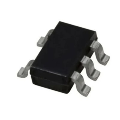
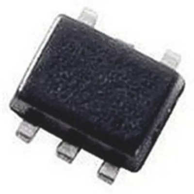
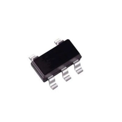
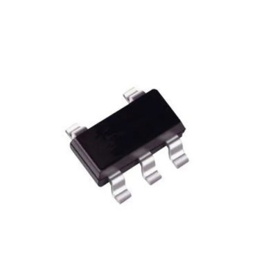
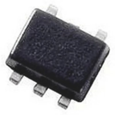
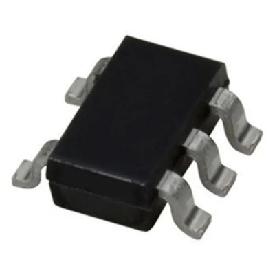
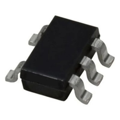
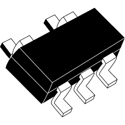
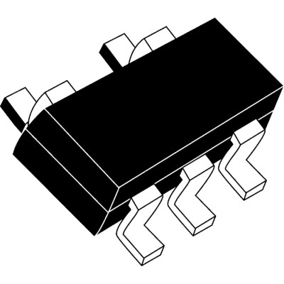
The device features a compact 3-pin SOT-89 surface mount package, enabling ease of integration into densely packed printed circuit boards while maintaining efficient heat dissipation. The low maximum drain-source resistance (Rds) of 180 mΩ contributes to reduced power loss and enhanced circuit efficiency.
Engineered to operate within a wide temperature range of -55°C to 150°C, the ZXMN3A01ZTA is suitable for industrial, consumer electronics, automotive, and telecommunications applications. Its maximum power dissipation of 2.12 W allows handling of significant thermal stresses in typical use cases.
The device exhibits a typical gate charge of 5 nC at gate-source voltage, facilitating fast switching operation, important in PWM controllers and switching power supplies. The capable gate voltage tolerance of -20 V to +20 V provides robustness against voltage spikes and ensures circuit reliability.
With precise construction, the MOSFET's physical dimensions are approximately 4.6 mm in length, 2.6 mm in width, and 1.6 mm in height, complying with standard surface mount package sizes suitable for automated manufacturing.
Maximum continuous drain current of 3.3 A. Maximum drain-source voltage of 30 V. Enhancement channel mode for controlled switching. 3-pin SOT-89 compact surface mount package. Low on-resistance of 180 mΩ for efficiency. 2.12 W maximum power dissipation.
Operating temperature range from -55°C to 150°C. Typical gate charge of 5 nC supporting fast switching. Gate-source voltage withstands -20 V to +20 V. Dimensions: 4.6 mm length, 2.6 mm width, 1.6 mm height.
This MOSFET is an excellent choice for electronic engineers designing circuits in industrial controls, power regulation systems, and automotive electronics requiring reliable N-channel MOSFETs with compact form factors and robust electrical characteristics.
Explore the wide range of semiconductor components at EnvMart to complement your electronic designs with trusted brands like DiodesZetex for enhanced performance and reliability.



 Global Payments 140+ Countries
 Global Shipping Fedex/UPS/DHL/Aramex/
BlueDart/Delhivery/DP World
 24/7 Customer Support Email/Chat/Telephonic Support
Comments (0)
Your review appreciation cannot be sent
Report comment
Report sent
Your report cannot be sent