$1.56
$1.51
Tax included

World's First Climate Tech Platform | Free Delivery in India | Global Shipping

Shop with confidence knowing that our 24/7 Customer Support is always available to assist with any inquiries

Avail maximum benefits from input tax mechanism on all your Business Invoices. Get GST Invoices on your business purchases. And 0% Taxes on all worldwide deliveries

If you find this product anywhere at lower cost than us. Call us and we will not only match the price but also give a complimentary coupon

Shop with assurance, as each product we offer is 100% original, ensuring quality and authenticity with every purchase
| Country of Origin | India |
|---|---|
| Brand | onsemi |
| Height | 9.19mm |
| Length | 10.16mm |
| Model | FQPF10N20C |
| Width | 4.7mm |
| Mount Type | Through Hole |
| Series | QFET |
| Maximum Operating Temperature | 150°C |
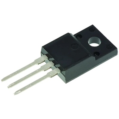
| Package Type | TO-220F |
| Minimum Operating Temperature | -55°C |
| Pin Count | 3 |
| Channel Type | N |
| Maximum Continuous Drain Current Id | 9.5A |
| Maximum Drain Source Voltage Vds | 200V |
| Maximum Drain Source Resistance Rds | 0.36Ω |
| Channel Mode | Enhancement |
| Maximum Power Dissipation Pd | 38W |
| Typical Gate Charge Qg @ Vgs | 20nC |
| Maximum Gate Source Voltage Vgs | -30, +30V |
| Forward Voltage Vf | 1.5V |
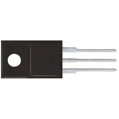
onsemi FQPF10N20C is an N-Channel QFET MOSFET transistor designed for high performance in power management and switching applications. It features enhancement mode operation, a maximum continuous drain current of 9.5 A, and a maximum drain-source voltage rating of 200 V. The device is housed in a 3-pin TO-220F through-hole package that supports robust mounting and electrical connections.
This MOSFET offers low on-state resistance of 0.36 Ohms which minimizes power losses during conduction. It also benefits from a typical gate charge of 20 nC, enhancing switching speeds and reducing switching losses. The component can safely dissipate up to 38 W of power under normal operating conditions.
It performs reliably over a wide temperature range from -55°C to 150°C, making it suitable for industrial, commercial, and automotive electronic systems. The maximum gate-source voltage rating ensures operational safety across varied voltage levels. This device finds use in power supplies, power factor correction circuits, DC-DC converters, plasma display panels, lighting ballasts, and motion control circuits.
Dimensions of length 10.16 mm, width 4.7 mm, and height 9.19 mm support compact circuit board layouts. The device does not carry any automotive certifications but complies with general semiconductor standards suitable for discrete applications.
Maximum continuous drain current of 9.5 A ensures high power handling capability. Supports a maximum drain-source voltage of 200 V for robust operation. Utilizes enhancement mode for reliable switching performance. Encapsulated in a durable TO-220F through-hole package with 3 pins.
Low maximum drain-source resistance of 0.36 Ohms reduces conduction loss. Typical gate charge of 20 nC improves switching efficiency and speed. Capable of dissipating up to 38 W power under rated conditions. Operating temperature range from -55°C to 150°C offers versatility in harsh environments.
Gate-source voltage max ratings of -30 V to +30 V provide operational safety margins. Compact dimensions optimize PCB footprint.
Ideal for use in industrial electronics, power conversion, renewable energy systems, and automotive electronic controls. Browse our semiconductor MOSFET catalog for related onsemi components and fully compatible power management products.
Review sent
Your review cannot be sent
Global Payments 140+ Countries

Global Shipping Fedex/UPS/DHL/Aramex/
BlueDart/Delhivery/DP World
24/7 Customer Support Email/Chat/Telephonic Support
Comments (0)
Your review appreciation cannot be sent
Report comment
Report sent
Your report cannot be sent