$1.18
$1.14
Tax included

World's First Climate Tech Platform | Free Delivery in India | Global Shipping

Shop with confidence knowing that our 24/7 Customer Support is always available to assist with any inquiries

Avail maximum benefits from input tax mechanism on all your Business Invoices. Get GST Invoices on your business purchases. And 0% Taxes on all worldwide deliveries

If you find this product anywhere at lower cost than us. Call us and we will not only match the price but also give a complimentary coupon

Shop with assurance, as each product we offer is 100% original, ensuring quality and authenticity with every purchase
| Country of Origin | Japan |
|---|---|
| Brand | Toshiba |
| Height | 2.3mm |
| Length | 6.5mm |
| Model | TK15S04N1L,LQ(O |
| Width | 5.5mm |
| Mount Type | Surface |
| Series | U-MOSVIII-H |
| Maximum Operating Temperature | 175°C |
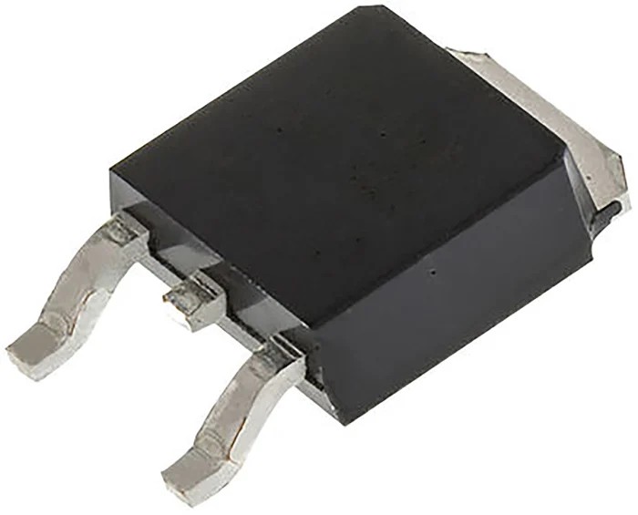
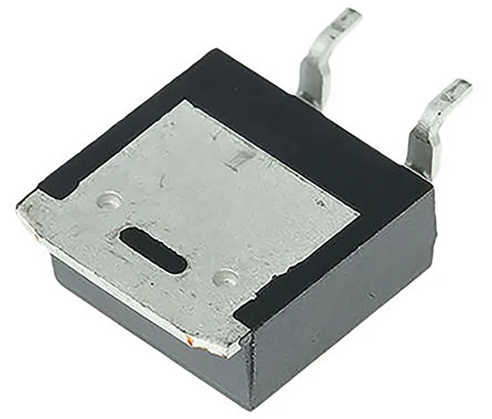
| Package Type | TO-252 |
| Pin Count | 3 |
| Channel Type | N |
| Maximum Continuous Drain Current Id | 15A |
| Maximum Drain Source Voltage Vds | 40V |
| Maximum Drain Source Resistance Rds | 37mΩ |
| Channel Mode | Enhancement |
| Maximum Power Dissipation Pd | 46W |
| Typical Gate Charge Qg @ Vgs | 10nC |
| Maximum Gate Source Voltage Vgs | -20, +20V |
| Forward Voltage Vf | -1.2V |
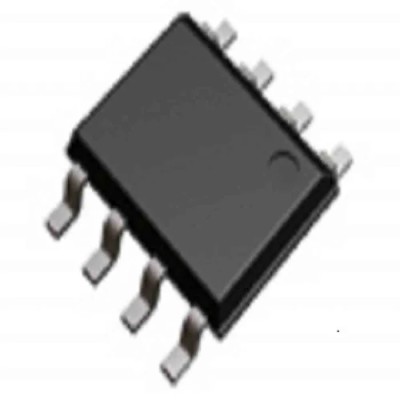
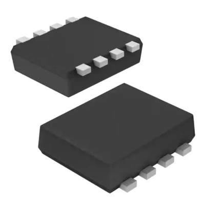
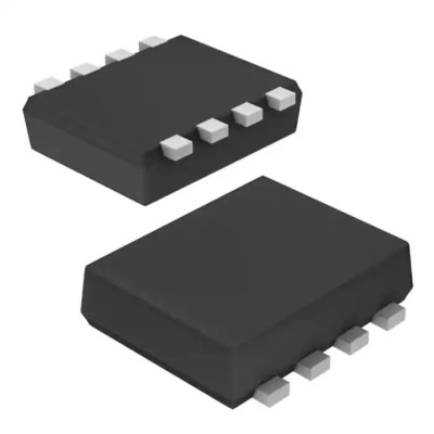
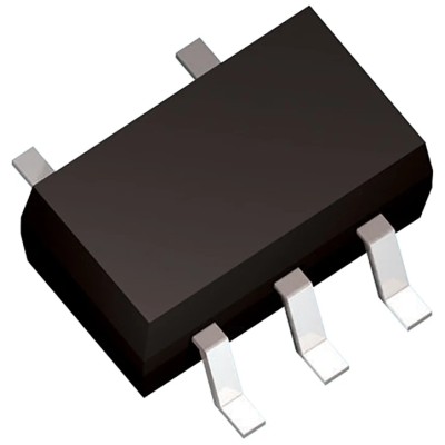
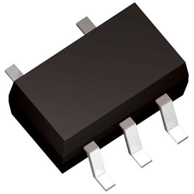
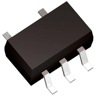
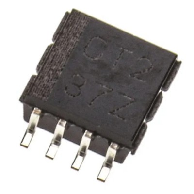
Toshiba TK15S04N1L,LQ(O is a U-MOSVIII-H series N-Channel Enhancement Mode power MOSFET, designed for surface mount applications requiring efficient power control and switching. Featuring a continuous drain current of 15 A and a maximum drain-source voltage of 40 V, it supports robust and reliable operation in various electronics and semiconductor device applications.
The 3-pin TO-252 package offers a compact footprint for modern PCB layouts. With a typical gate charge of just 10 nC at 10 V, this MOSFET supports rapid switching performance while minimizing power loss. The low maximum drain-source resistance of 37 milliohms reduces conduction losses, improving overall system efficiency.
Operating safely at temperatures up to 175°C, this device is well suited for demanding industrial and commercial environments such as power supplies, motor drives, and general-purpose power management in electronic circuits. It supports a maximum gate-source voltage range of -20 V to +20 V for flexible gate drive designs.
Physical dimensions are 6.5 mm length, 5.5 mm width, and 2.3 mm height, making integration into compact assemblies straightforward. Despite the compact size, the MOSFET can dissipate up to 46 watts of power, enabling high-performance applications.
Enhancement mode N-Channel MOSFET with 15 A continuous drain current rating. Maximum drain-source voltage of 40 V ensuring solid switching capability. Compact 3-pin TO-252 surface-mount package for space-saving design. Low on-resistance of 37 milliohms for efficient conduction.
Maximum power dissipation capacity of 46 watts. Wide allowable gate-source voltage range from -20 V to +20 V. Typical gate charge of 10 nanocoulombs enhances switching efficiency. Forward voltage of -1.2 V suitable for effective switching.
Designed to operate up to 175°C in harsh environments. Manufactured in Japan ensuring high quality standards.
This Toshiba MOSFET is ideal for industrial, power management, consumer electronics, and automotive electronics use cases, where efficient power switching and thermal robustness are critical. It suits applications such as motor drives, power supply units, DC-DC converters, and electronic load switching.
Explore related power semiconductor components and electronic parts in EnvMart's Electronics & Electricals category for matching system and design requirements.
Review sent
Your review cannot be sent
Global Payments 140+ Countries
Global Shipping Fedex/UPS/DHL/Aramex/
BlueDart/Delhivery/DP World
24/7 Customer Support Email/Chat/Telephonic Support
Comments (0)
Your review appreciation cannot be sent
Report comment
Report sent
Your report cannot be sent