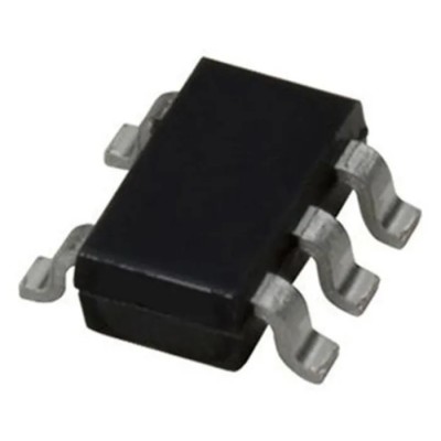
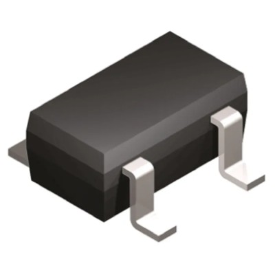
$0.40
$0.39
Tax included

World's First Climate Tech Platform | Free Delivery in India | Global Shipping

Shop with confidence knowing that our 24/7 Customer Support is always available to assist with any inquiries

Avail maximum benefits from input tax mechanism on all your Business Invoices. Get GST Invoices on your business purchases. And 0% Taxes on all worldwide deliveries

If you find this product anywhere at lower cost than us. Call us and we will not only match the price but also give a complimentary coupon

Shop with assurance, as each product we offer is 100% original, ensuring quality and authenticity with every purchase
| Country of Origin | India |
|---|---|
| Brand | onsemi |
| Height | 1.5mm |
| Length | 5mm |
| Model | FDS4685 |
| Width | 4mm |
| Mount Type | Surface |
| Series | PowerTrench |
| Maximum Operating Temperature | 150°C |
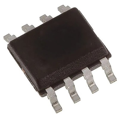
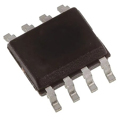
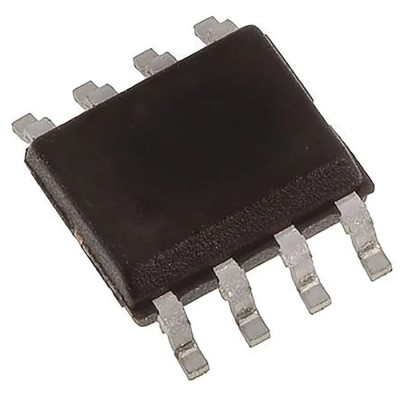
| Package Type | SOIC |
| Minimum Operating Temperature | -55°C |
| Pin Count | 8 |
| Channel Type | Type P |
| Maximum Continuous Drain Current Id | 8.2A |
| Maximum Drain Source Voltage Vds | 40V |
| Maximum Drain Source Resistance Rds | 27mΩ |
| Channel Mode | Enhancement |
| Maximum Power Dissipation Pd | 2.5W |
| Typical Gate Charge Qg @ Vgs | 19nC |
| Maximum Gate Source Voltage Vgs | -20, +20V |
| Forward Voltage Vf | -1.2V |
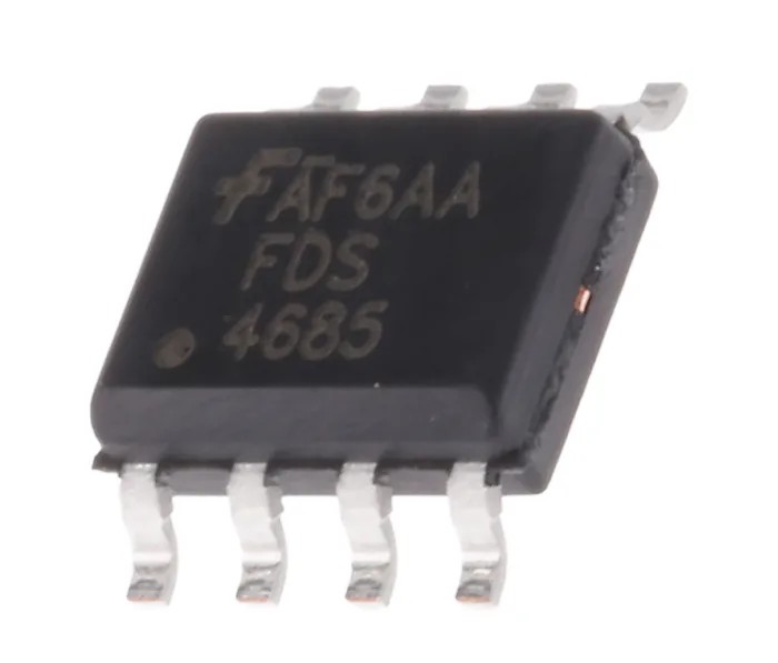
onsemi FDS4685 PowerTrench Type P-Channel MOSFET is a high-performance semiconductor device designed for efficient power switching in electronic circuits. With a continuous drain current rating of 8.2 A and a maximum drain-source voltage of 40 V, this MOSFET supports a wide range of applications in power management and switching.
The PowerTrench technology integrates a shielded-gate structure that improves charge balance and minimizes the figure of merit (FOM) for superior switching efficiency. Its low on-resistance (27 mΩ max) reduces conduction losses, making it ideal for synchronous rectification in AC/DC power supplies and other power conversion systems.
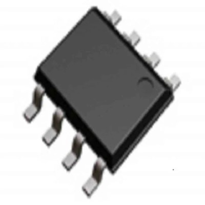
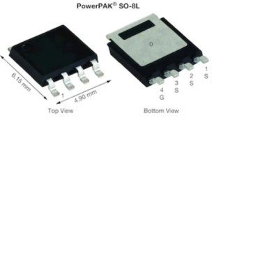
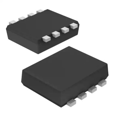
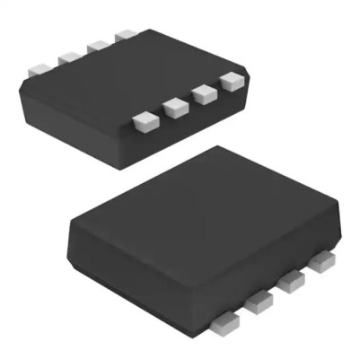
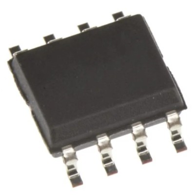
The device is housed in an 8-pin SOIC surface-mount package with compact dimensions (5 mm × 4 mm × 1.5 mm), allowing for space-saving PCB designs. The enhancement mode channel with a gate charge of 19 nC facilitates fast switching and low power dissipation (2.5 W max).
Designed to operate reliably across wide temperatures from -55°C to 150°C, this MOSFET suits industrial, automotive (non-automotive standard), and commercial applications where stable and efficient power handling is essential. The maximum gate-source voltage tolerance of ±20 V expands its compatibility with various gate driver circuits.
Key features such as the soft reverse recovery body diode aid in eliminating the need for snubber circuits and enable replacement of higher voltage MOSFETs, improving system efficiency and simplifying design.
The device’s advanced PowerTrench technology delivers excellent switching speed and efficiency. Its compact small-outline integrated circuit (SOIC) package supports surface mount assembly. Operating temperature range from -55°C up to 150°C ensures broad application scope.
Maximum drain-source voltage of 40 V and continuous drain current of 8.2 A suits diverse power applications. Typical gate charge of 19 nC leads to reduced switching losses in high-frequency circuits. Robust gate-source voltage handling at ±20 V adds protection and flexibility in circuit design.
This onsemi MOSFET is perfect for use in power supplies, industrial automation, consumer electronics, and telecommunications equipment. Its efficiency and performance characteristics support both design efficiency and long-term operational reliability.
Explore more high-quality semiconductors and power device solutions at EnvMart to meet your industrial and commercial requirements.
Review sent
Your review cannot be sent
Global Payments 140+ Countries

Global Shipping Fedex/UPS/DHL/Aramex/
BlueDart/Delhivery/DP World
24/7 Customer Support Email/Chat/Telephonic Support
Comments (0)
Your review appreciation cannot be sent
Report comment
Report sent
Your report cannot be sent