$3.01
$2.92
Tax included

World's First Climate Tech Platform | Free Delivery in India | Global Shipping

Shop with confidence knowing that our 24/7 Customer Support is always available to assist with any inquiries

Avail maximum benefits from input tax mechanism on all your Business Invoices. Get GST Invoices on your business purchases. And 0% Taxes on all worldwide deliveries

If you find this product anywhere at lower cost than us. Call us and we will not only match the price but also give a complimentary coupon

Shop with assurance, as each product we offer is 100% original, ensuring quality and authenticity with every purchase
| Country of Origin | China |
|---|---|
| Brand | onsemi |
| Height | 16.3mm |
| Length | 10.67mm |
| Model | FCP190N65S3 |
| Width | 4.7mm |
| Mount Type | Through Hole |
| Series | SuperFET II |
| Maximum Operating Temperature | 150°C |
| Package Type | TO-220 |
| Minimum Operating Temperature | -55°C |
| Pin Count | 3 |
| Channel Type | N |
| Maximum Continuous Drain Current Id | 17A |
| Maximum Drain Source Voltage Vds | 650V |
| Maximum Drain Source Resistance Rds | 190mΩ |
| Channel Mode | Enhancement |
| Maximum Power Dissipation Pd | 144W |
| Typical Gate Charge Qg @ Vgs | 33nC |
| Maximum Gate Source Voltage Vgs | 30V |
| Forward Voltage Vf | 1.2V |
| Internal Gate Resistance | 7.0 ohm |
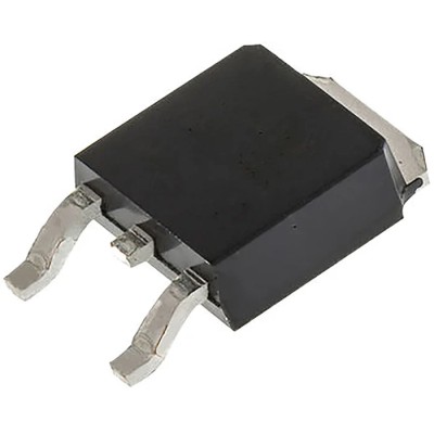
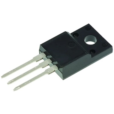
onsemi FCP190N65S3 is a SuperFET II N-Channel MOSFET engineered for high voltage and current power switching applications. It supports a continuous drain current up to 17 amperes and withstands up to 650 volts across the drain-source terminals, packaged in a reliable 3-pin TO-220 format suited for through-hole mounting.
This MOSFET utilizes advanced SuperFET II charge balance technology that significantly reduces conduction and switching losses, enabling improved system efficiency and miniaturization in industrial power electronics.
Operating temperatures range from -55°C to 150°C, allowing use in harsh environments. The device features a maximum power dissipation of 144 watts, supporting heavy load conditions. Its typical gate charge of 33 nC and low effective output capacitance contribute to superior switching performance, limiting power losses during operation.
The SuperFET II design incorporates internal gate resistance of 7.0 ohms to reduce voltage oscillations during switching events, enhancing reliability and noise performance. The typical forward voltage is 1.2 V, representing efficient conduction at nominal operational currents.
The 3-pin TO-220 package facilitates simple through-hole mounting and effective thermal dissipation. Low Rds(on) of 190 milliohms reduces conduction losses and enhances current capacity. Wide operational temperature range for industrial and commercial electronic power systems.
SuperFET II technology minimizes switching losses for power-efficient designs. Robust maximum power dissipation rating supports demanding applications. Internal gate resistance improves switching stability and reduces electromagnetic interference.
Designed for use in power management, automotive electronics, and energy conversion systems. Manufactured in China, ensuring quality control and consistent performance. This MOSFET is ideal for industrial, automotive, HVAC, manufacturing, and power supply applications requiring efficient, high voltage switching components.
Explore more semiconductor devices and MOSFETs on EnvMart for advanced power electronics solutions.
Review sent
Your review cannot be sent
Global Payments 140+ Countries

Global Shipping Fedex/UPS/DHL/Aramex/
BlueDart/Delhivery/DP World
24/7 Customer Support Email/Chat/Telephonic Support
Comments (0)
Your review appreciation cannot be sent
Report comment
Report sent
Your report cannot be sent