$0.37
$0.36
Tax included

World's First Climate Tech Platform | Free Delivery in India | Global Shipping

Shop with confidence knowing that our 24/7 Customer Support is always available to assist with any inquiries

Avail maximum benefits from input tax mechanism on all your Business Invoices. Get GST Invoices on your business purchases. And 0% Taxes on all worldwide deliveries

If you find this product anywhere at lower cost than us. Call us and we will not only match the price but also give a complimentary coupon

Shop with assurance, as each product we offer is 100% original, ensuring quality and authenticity with every purchase
| Country of Origin | India |
|---|---|
| Brand | onsemi |
| Height | 1mm |
| Length | 3mm |
| Model | FDC6306P |
| Width | 1.7mm |
| Mount Type | Surface |
| Series | PowerTrench |
| Maximum Operating Temperature | 150°C |
| Package Type | SOT-23 |
| Minimum Operating Temperature | -55°C |
| Pin Count | 6 |
| Number of Elements per Chip | 2 |
| Channel Type | Type P |
| Maximum Continuous Drain Current Id | 1.9A |
| Maximum Drain Source Voltage Vds | 20V |
| Maximum Drain Source Resistance Rds | 270mΩ |
| Channel Mode | Enhancement |
| Maximum Power Dissipation Pd | 960mW |
| Typical Gate Charge Qg @ Vgs | 3nC |
| Maximum Gate Source Voltage Vgs | -8, +8V |
| Forward Voltage Vf | -0.8V |
| Transistor Configuration | Isolated |
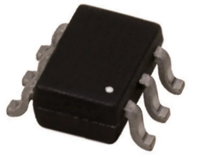
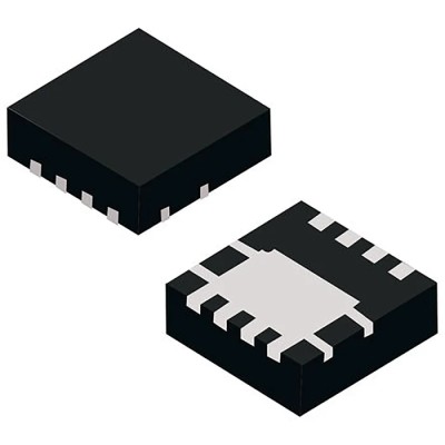
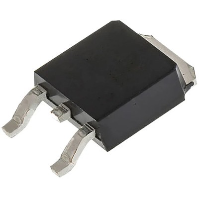
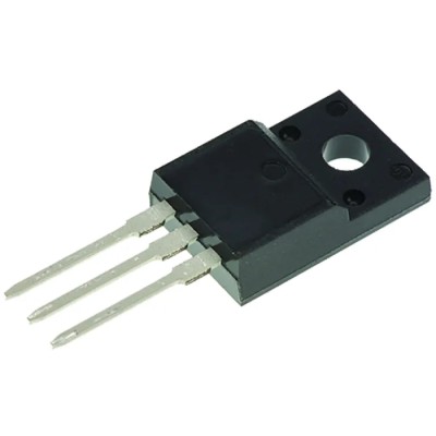
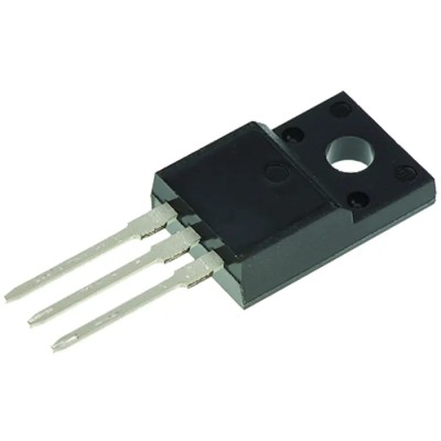
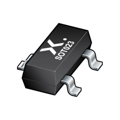
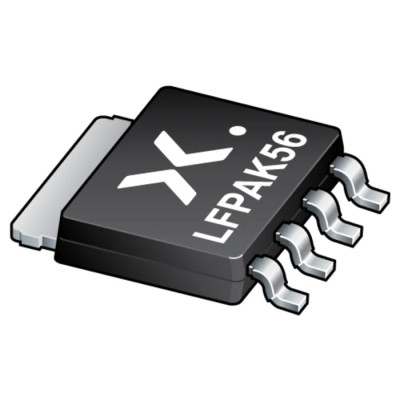
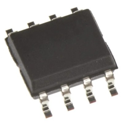
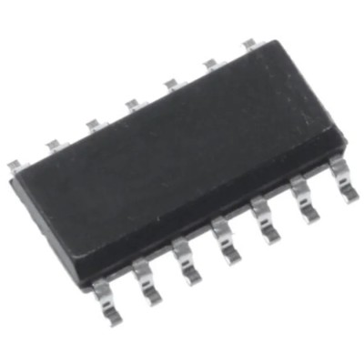
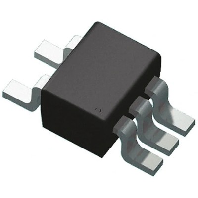
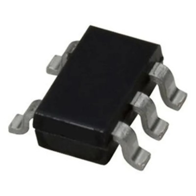
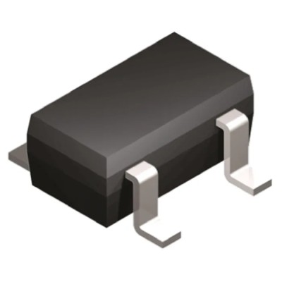
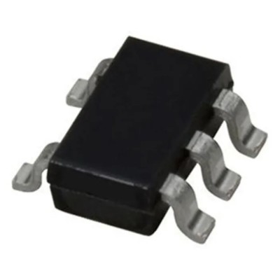
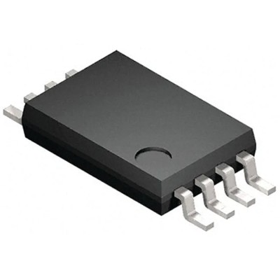
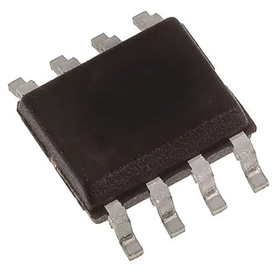
onsemi FDC6306P is an Isolated PowerTrench 2 Type P-Channel MOSFET providing a maximum continuous drain current of 1.9 A and maximum drain-source voltage of 20 V in a compact SOT-23 6-pin surface mount package. This device employs an enhancement channel mode with isolated transistor configuration designed for efficient power switching applications.
PowerTrench® MOSFETs from onsemi are optimised for high system efficiency and increased power density by combining low gate charge, low reverse recovery charge, and soft reverse recovery body diode for fast synchronous rectification, widely used in AC/DC power supplies, industrial, and manufacturing electronic circuits.
The FDC6306P features a shielded-gate structure offering charge balance, resulting in significantly improved Figure of Merit (FOM) compared to previous generation MOSFETs. Its soft body diode enhances efficiency by eliminating the need for snubber circuits or higher voltage MOSFET replacements.
Operating temperature range from -55°C to 150°C and maximum power dissipation of 960 mW support demanding industrial and commercial electronic designs requiring robust thermal and electrical performance.
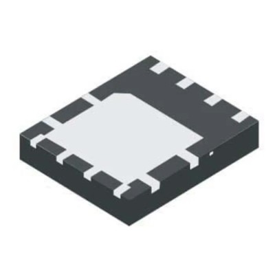
With compact physical dimensions of 3 mm length, 1.7 mm width, and 1 mm height, this device is well suited for space-conscious electronic component integration while maintaining reliable surface mounting with 6 pins.
The MOSFET offers low typical gate charge of 3 nC to facilitate fast switching. Maximum gate-source voltage values of -8 V to +8 V ensure device protection during operation. The device includes two elements per chip offering enhanced dual transistor configuration.
Applications include power management in industrial, manufacturing, and consumer electronic devices where efficient switching MOSFETs with compact packages are essential.
onsemi provides a comprehensive range of MOSFET devices contoured for various voltage and current ratings including high-voltage and low-voltage options to meet diverse engineering requirements.
Explore similar Semiconductor and MOSFET products to find the best solutions for your current and future project needs at EnvMart.
Review sent
Your review cannot be sent
Global Payments 140+ Countries

Global Shipping Fedex/UPS/DHL/Aramex/
BlueDart/Delhivery/DP World
24/7 Customer Support Email/Chat/Telephonic Support
Comments (0)
Your review appreciation cannot be sent
Report comment
Report sent
Your report cannot be sent