$2.09
$2.02
Tax included

World's First Climate Tech Platform | Free Delivery in India | Global Shipping

Shop with confidence knowing that our 24/7 Customer Support is always available to assist with any inquiries

Avail maximum benefits from input tax mechanism on all your Business Invoices. Get GST Invoices on your business purchases. And 0% Taxes on all worldwide deliveries

If you find this product anywhere at lower cost than us. Call us and we will not only match the price but also give a complimentary coupon

Shop with assurance, as each product we offer is 100% original, ensuring quality and authenticity with every purchase
| Country of Origin | India |
|---|---|
| Brand | onsemi |
| Height | 4.83mm |
| Length | 10.67mm |
| Model | FDB33N25TM |
| Width | 11.33mm |
| Mount Type | Surface |
| Series | UniFET |
| Maximum Operating Temperature | 150°C |
| Package Type | TO-263 |
| Minimum Operating Temperature | -55°C |
| Pin Count | 3 |
| Channel Type | N |
| Maximum Continuous Drain Current Id | 33A |
| Maximum Drain Source Voltage Vds | 250V |
| Maximum Drain Source Resistance Rds | 94mΩ |
| Channel Mode | Enhancement |
| Maximum Power Dissipation Pd | 235W |
| Typical Gate Charge Qg @ Vgs | 36.8nC |
| Maximum Gate Source Voltage Vgs | -30, +30V |
| Forward Voltage Vf | 1.4V |
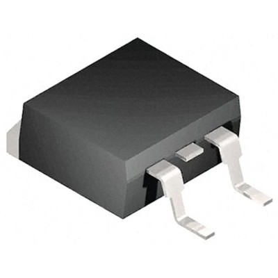
onsemi FDB33N25TM is a UniFET N-Channel Enhancement Mode MOSFET designed for high voltage power switching applications. It features a maximum continuous drain current of 33 A and a drain-source voltage rating of 250 V, housed in a compact 3-pin TO-263 package suitable for surface mounting.
The MOSFET provides low on-state resistance of 94 milliohms, contributing to its efficient switching and power dissipation capability rated at 235 W. Its typical gate charge of 36.8 nC at 10 V ensures responsive switching behavior. The device can operate reliably within a wide temperature range of -55°C to 150°C, making it suitable for harsh industrial environments.
onsemi's UniFET technology integrates an internal gate-source ESD diode that allows the MOSFET to withstand electrostatic discharge events exceeding 2000 V HBM, enhancing reliability in demanding electronic circuits.
This MOSFET is suitable for a variety of industrial and commercial semiconductor applications, notably switching power converter designs such as power factor correction modules, flat panel displays, ATX power supplies, and electronic lamp ballasts.
Maximum continuous drain current: 33 A. Maximum drain-source voltage rating: 250 V. Low on-resistance: 94 mΩ. Power dissipation: 235 W. Package: Surface mount TO-263, 3-pin. Operating temperature: -55°C to 150°C. Typical gate charge: 36.8 nC at Vgs=10 V.
Internal gate-source ESD protection diode. Enhancement mode channel. Dimensions: Height 4.83 mm, Length 10.67 mm, Width 11.33 mm.
Whether for industrial power management, electronics manufacturing, or HVAC controls, the FDB33N25TM MOSFET delivers reliable performance and durability. Explore more semiconductor components on EnvMart for your electronics projects and applications.
Explore more products in our Discrete Semiconductor category.
Review sent
Your review cannot be sent
Global Payments 140+ Countries
Global Shipping Fedex/UPS/DHL/Aramex/
BlueDart/Delhivery/DP World
24/7 Customer Support Email/Chat/Telephonic Support
Comments (0)
Your review appreciation cannot be sent
Report comment
Report sent
Your report cannot be sent