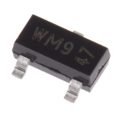
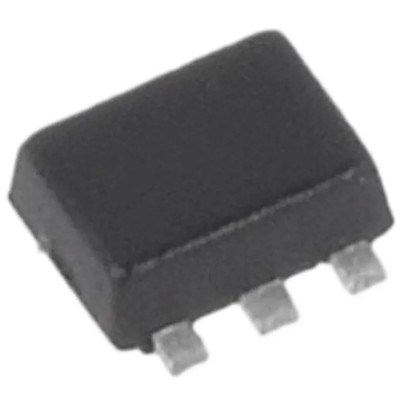
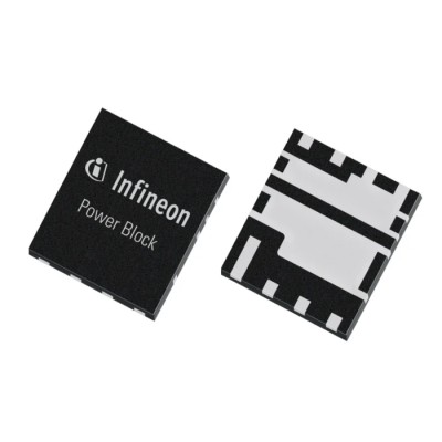
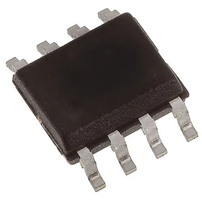
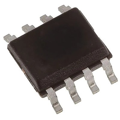
The Infineon OptiMOS 2 BSL316CH6327XTSA1 is an advanced dual N, P-Channel MOSFET engineered for precise, low-voltage switching in automotive, industrial, and control system applications. Designed with isolated topology, this MOSFET delivers both N- and P-channel elements within a single surface-mount TSOP-6 package, making it ideal where board space and reliable power management are critical.
With a 1.5A continuous drain current and a maximum drain-source voltage of 30V, this device is well suited for DC load switching in vehicle electronics, battery management, and protection circuits. The enhancement mode ensures rapid ON/OFF performance, while its low drain-source resistance (280mΩ) reduces energy dissipation and optimizes system efficiency.
Automotive environments demand robust electronic components. BSL316CH6327XTSA1 withstands temperatures from −55°C up to 150°C, ensuring stable operation in extreme conditions. Its 2.4nC typical gate charge also supports efficient gate drive and high-speed switching, essential for modern power supplies and driver stages.
Dual isolated N-channel and P-channel MOSFET design for flexible deployment. Delivers a maximum power dissipation up to 500mW to prevent thermal overload. 6-pin TSOP-6 enclosure minimizes PCB footprint for dense layouts.
AEC-Q101 certification demonstrates proven reliability for automotive use cases. Suitable for SMD power management, push-pull drivers, load disconnects, and temperature-sensitive circuitry. 2 elements per chip enable efficient complementary switching within compact modules.
Whether you are engineering battery protection modules, smart vehicle electronics, or robust industrial controllers, the Infineon BSL316CH6327XTSA1 provides the electrical and mechanical characteristics required for demanding switching functions. Each device offers precision switching, thermal stability, and surface-mount simplicity.
Typical applications are found in automotive modules, factory automation, DC-DC conversion, and high-efficiency SMD power switching on control boards. Its compact size is particularly advantageous in densely populated PCBs where thermal management, reliability, and form-factor matter.
Explore more MOSFETs, power semiconductors, and automotive-grade solutions under the Infineon brand in the EnvMart Electronics & Electricals catalogue.





 Global Payments 140+ Countries
 Global Shipping Fedex/UPS/DHL/Aramex/
BlueDart/Delhivery/DP World
Global Shipping Fedex/UPS/DHL/Aramex/
BlueDart/Delhivery/DP World 24/7 Customer Support Email/Chat/Telephonic Support
Comments (0)
Your review appreciation cannot be sent
Report comment
Report sent
Your report cannot be sent