
$0.14
$0.13
-3%
New
World's First Climate Tech Platform | Free Delivery in India | Global Shipping

Shop with confidence knowing that our 24/7 Customer Support is always available to assist with any inquiries

Avail maximum benefits from input tax mechanism on all your Business Invoices. Get GST Invoices on your business purchases. And 0% Taxes on all worldwide deliveries

If you find this product anywhere at lower cost than us. Call us and we will not only match the price but also give a complimentary coupon

Shop with assurance, as each product we offer is 100% original, ensuring quality and authenticity with every purchase
| Country of Origin | China |
|---|---|
| Brand | onsemi |
| Height | 0.6mm |
| Length | 1.7mm |
| Model | NTZD3154NT1G |
| Width | 1.3mm |
| Mount Type | Surface |
| Maximum Operating Temperature | 150°C |
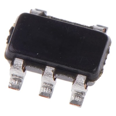
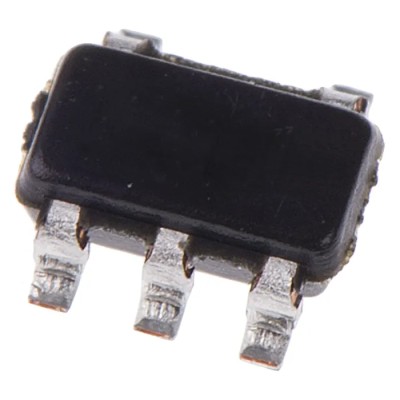
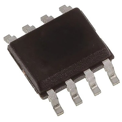
| Package Type | SOT-563 |
| Minimum Operating Temperature | -55°C |
| Pin Count | 6 |
| Number of Elements per Chip | 2 |
| Channel Type | Type N |
| Maximum Continuous Drain Current Id | 540mA |
| Maximum Drain Source Voltage Vds | 20V |
| Maximum Drain Source Resistance Rds | 900mΩ |
| Channel Mode | Enhancement |
| Maximum Power Dissipation Pd | 250mW |
| Typical Gate Charge Qg @ Vgs | 1.5nC |
| Maximum Gate Source Voltage Vgs | 7V |
| Forward Voltage Vf | 0.7V |
| Transistor Configuration | Dual |
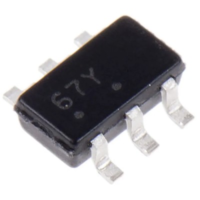
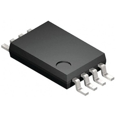
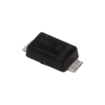
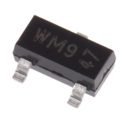
The onsemi NTZD3154NT1G Dual N-Channel Small Signal MOSFET is a high-performance semiconductor device engineered for modern electronic circuits requiring efficient switching and low power loss. Featuring enhancement mode operation and two N-channel MOSFETs on one chip, this model is designed for applications such as load and power switches, converter circuits, and battery management.
With a maximum continuous drain current of 540 mA and a maximum drain source voltage of 20 V, the NTZD3154NT1G delivers reliable performance for low to moderate power switching tasks. Its compact SOT-563 surface-mount package, measuring just 1.7 mm in length, 1.3 mm in width, and 0.6 mm in height, helps engineers achieve dense PCB layouts and miniaturize designs without sacrificing electrical characteristics.
System efficiency is improved thanks to the low maximum drain source resistance of just 900 mΩ, which minimizes heat generation during operation. The enhancement channel mode ensures precise control of the device, while a typical gate charge of 1.5 nC at Vgs enables fast switching responses vital in converter and power management systems. The dual transistor configuration provides flexibility in circuit design by allowing independent or paired operation.
This MOSFET is rated for a maximum power dissipation of 250 mW, making it suitable for portable devices and compact applications. It operates reliably within a wide temperature range from -55°C up to 150°C, supporting industrial, commercial, and harsh-environment electronics.
Additional features include forward voltage (Vf) of 0.7 V and maximum gate source voltage (Vgs) of 7 V. ESD protection for the gate makes NTZD3154NT1G valuable for battery-powered designs and sensitive switching applications.
Ideal use cases include load/power switches, converter circuits in power supply designs, and battery management in consumer, industrial, and automotive electronics. The device is compliant with standard quality requirements and does not adhere to a specific automotive standard.
For specialized MOSFETs and semiconductor solutions, explore more options from the 'onsemi' brand in the MOSFETs category at EnvMart.
Review sent
Your review cannot be sent
Interested in this product? Drop us an email and we will let you know when it's available for order.
Global Payments 140+ Countries
Global Shipping Fedex/UPS/DHL/Aramex/
BlueDart/Delhivery/DP World
24/7 Customer Support Email/Chat/Telephonic SupportInterested in this product? Drop us an email and we will let you know when it's available for order.
Comments (0)
Your review appreciation cannot be sent
Report comment
Report sent
Your report cannot be sent