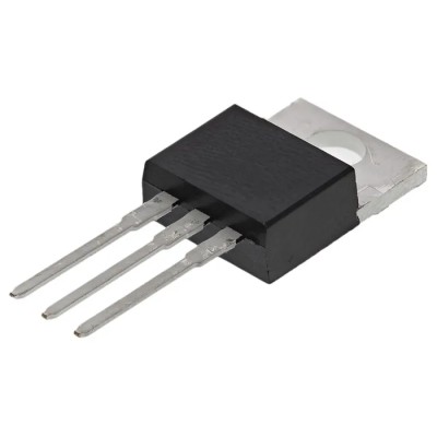
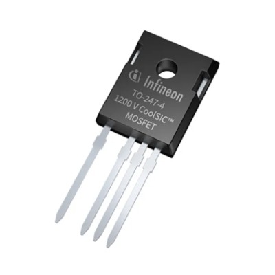
Infineon IPW60R160C6FKSA1 CoolMOS C6 N-Channel Power Transistor is a high-performance device rated for 23.8 A maximum continuous drain current and withstands 600 V drain-source voltage with enhancement mode operation. Packaged in a robust 3-pin TO-247 form factor for through-hole mounting, it is ideal for industrial electronic applications requiring reliable power management.
This transistor supports a maximum power dissipation of 176 W, allowing for efficient heat handling in demanding environments. Its operational temperature range from -55°C to 150°C makes it suitable for various industrial and automotive applications where thermal stability is critical.
The device boasts a typical gate charge of 75 nC at the gate-source voltage, enabling rapid switching and improved overall efficiency in power conversion circuits. The low maximum on-resistance of 0.16 Ω minimizes power losses, which is essential for energy-efficient designs.
With a forward voltage of 0.9 V, the transistor ensures minimal voltage drop while operating under load, saving energy. It tolerates a maximum gate-source voltage of ±30 V, providing protection against voltage spikes during switching events.
This product complies with the JEDEC J-STD20 and JESD22 reliability standards and features Pb-free plating, meeting modern environmental and safety requirements. Typical use cases include industrial power supplies, motor control, solar inverters, and other applications requiring high-efficiency power switching.
The package dimensions are width 5.21 mm, height 21.1 mm, and length 16.13 mm, facilitating easy integration with standard heatsinks and PCBs. Explore more power semiconductors and MOSFET devices in the Electronics & Electricals category on EnvMart to optimize your applications.
This power transistor features enhancement mode operation for efficient switching. It includes a 3-pin TO-247 through-hole package suitable for robust mounting. The device supports a maximum power dissipation of 176 W. Operating temperature ranges from -55°C minimum to 150°C maximum ensure durability.
The typical gate charge is 75 nC at Vgs, optimizing switching performance. Maximum drain-source resistance is 0.16 ohms, reducing conduction losses. Forward voltage is 0.9 V, contributing to low voltage drops under load.
Maximum gate-source voltage tolerance is ±30 V, ensuring safe gate control. Complies with JEDEC J-STD20 and JESD22 standards and features Pb-free plating. Discover the advanced portfolio of Infineon Power MOSFETs on EnvMart for industrial, automotive, and commercial applications.






Comments (0)
Your review appreciation cannot be sent
Report comment
Report sent
Your report cannot be sent