onsemi NTZD3152PT1G is a dual isolated 2 type P-channel small signal MOSFET designed for efficient, reliable switching operations in electronic circuits. This MOSFET features an enhancement mode channel with a maximum continuous drain current of 430 mA and a maximum drain-source voltage rating of 20 V, making it suitable for low power electronic component applications.
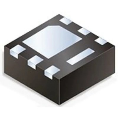
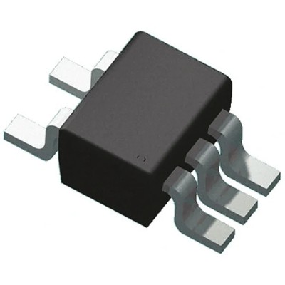
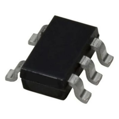
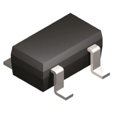
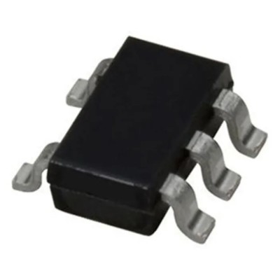
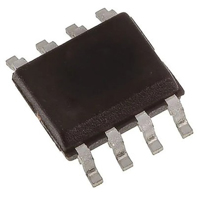
The device comes in a space-saving 6-pin SOT-563 surface mount package, ideal for modern compact electronics requiring minimal board space. Operating temperature spans from -55°C to +150°C, supporting use in demanding environments.
Key electrical characteristics include a maximum power dissipation of 280 mW, typical gate charge of 10 nC to facilitate rapid switching, and a maximum drain-source resistance of 2 Ω to reduce conduction losses. Its maximum gate-source voltage is ±6 V, enhancing input resilience.
This MOSFET also features a forward voltage drop of -0.8 V, and contains two elements per chip, offering dual transistor configuration within a single package. Its compact physical dimensions - 1.7 mm length, 1.3 mm width, and 0.6 mm height - permit integration into high-density PCB layouts for industrial, automotive, and consumer electronic applications.
Applications include discrete semiconductor switching, small signal amplification, and general purpose low power electronic devices in industrial control, communication equipment, and automotive electronics. The NTZD3152PT1G is manufactured to meet industry standards for quality and reliability, though no specific automotive certifications apply to this model.
This product supports thorough design integration with provided technical documentation and is suited for surface mount technology assembly lines, facilitating efficient manufacturing workflows.
The device features enhancement mode channel operation for efficient switching. It comes in a compact 6-pin SOT-563 surface mount package. Maximum continuous drain current is 430 mA, suitable for small signal applications.
Maximum power dissipation is rated at 280 mW ensuring reliable operation. Operating temperature ranges from -55°C to +150°C for wide environmental compatibility. Low typical gate charge of 10 nC optimizes switching speed and power loss.
Maximum drain-source resistance is 2 Ω for improved conduction. Maximum gate-source voltage tolerates ±6 V providing input protection. Compact chip dimensions enable dense PCB layouts. Explore more semiconductor components and MOSFET transistors at EnvMart to fulfill your industrial, laboratory, automotive, and communications electronic needs.






Comments (0)
Your review appreciation cannot be sent
Report comment
Report sent
Your report cannot be sent