$0.82
$0.80
Tax included

World's First Climate Tech Platform | Free Delivery in India | Global Shipping

Shop with confidence knowing that our 24/7 Customer Support is always available to assist with any inquiries

Avail maximum benefits from input tax mechanism on all your Business Invoices. Get GST Invoices on your business purchases. And 0% Taxes on all worldwide deliveries

If you find this product anywhere at lower cost than us. Call us and we will not only match the price but also give a complimentary coupon

Shop with assurance, as each product we offer is 100% original, ensuring quality and authenticity with every purchase
| Country of Origin | India |
|---|---|
| Brand | onsemi |
| Height | 1.7mm |
| Length | 3.7mm |
| Model | FDT86113LZ |
| Width | 6.7mm |
| Mount Type | Surface |
| Series | PowerTrench |
| Maximum Operating Temperature | 150°C |
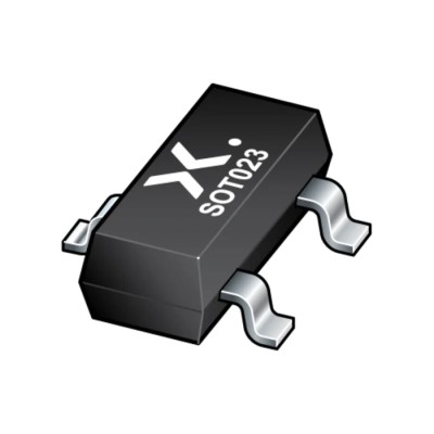
| Package Type | SOT-223 |
| Minimum Operating Temperature | -55°C |
| Pin Count | 4 |
| Channel Type | N |
| Maximum Continuous Drain Current Id | 3.3A |
| Maximum Drain Source Voltage Vds | 100V |
| Maximum Drain Source Resistance Rds | 189mΩ |
| Channel Mode | Enhancement |
| Maximum Power Dissipation Pd | 2.2W |
| Typical Gate Charge Qg @ Vgs | 4.1nC |
| Maximum Gate Source Voltage Vgs | -20, +20V |
| Forward Voltage Vf | 1.3V |
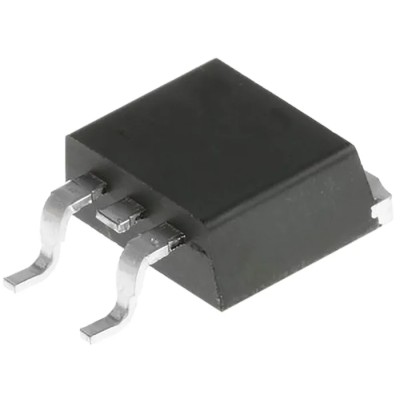
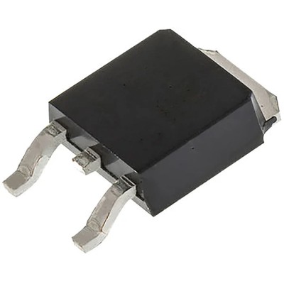
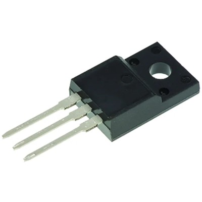
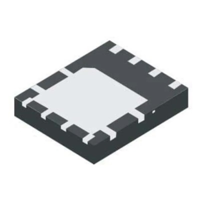
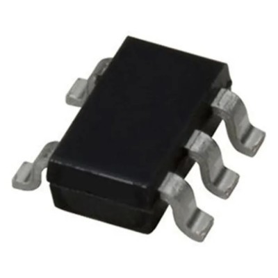
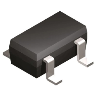
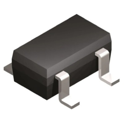
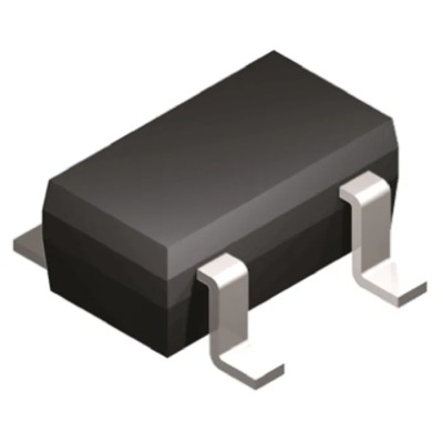
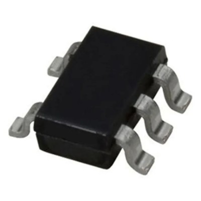
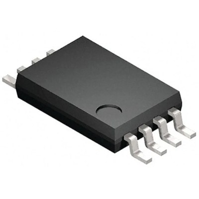
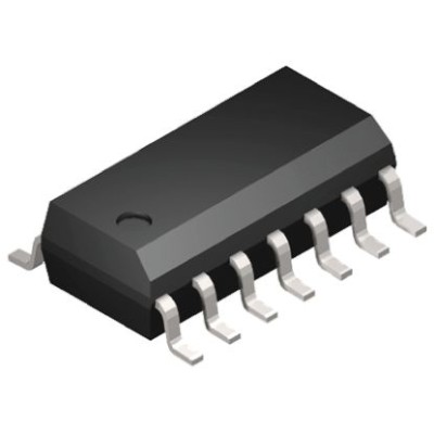
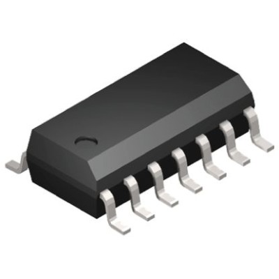
The onsemi FDT86113LZ is a PowerTrench® N-Channel MOSFET designed for high-performance power switching and amplification applications. It supports a continuous drain current of 3.3 A and a maximum drain-source voltage of 100 V. Packaged in a 4-pin SOT-223 surface mount device, this MOSFET offers compact size with dimensions of 3.7 mm length, 6.7 mm width, and 1.7 mm height, making it suitable for space-constrained electronic designs.
Operating efficiently in enhancement mode, this transistor ensures low on-resistance at 189 milliohms maximum, contributing to reduced power dissipation up to 2.2 W. Its gate charge of 4.1 nC at rated gate voltage facilitates quick switching, essential for high-frequency power management and switching power supplies.
The device withstands operating temperatures from -55°C to 150°C, ensuring reliability under harsh environments commonly found in industrial and consumer electronics. Its maximum gate-source voltage rating of ±20 V provides robust protection to the gate terminal, enhancing device stability over its operational lifecycle.
Typical forward voltage drop of 1.3 V assures predictable voltage characteristics in circuit applications. With a 4-pin footprint optimized for surface mounting, integration on printed circuit boards is straightforward, allowing for compact and efficient designs.
Common applications of the FDT86113LZ include power supply regulation, DC-DC conversion, load switching, and amplification within electronic circuits used in industrial, commercial, and consumer device contexts.
Designed for surface mounting in electronic circuits with SOT-223 package type. Features enhancement mode operation for efficient switching. Maximum drain-source resistance of 189 milliohms ensures low power losses. Operates reliably between -55°C and 150°C for diverse environments.
Maximum power dissipation rating of 2.2 W supports moderate power applications. Typical gate charge of 4.1 nC enables fast switching speeds. Forward voltage drop approximately 1.3 V under rated conditions. Pin count of 4 facilitates straightforward PCB integration.
High maximum gate-source voltage tolerance of ±20 V safeguards gate integrity. Explore more onsemi semiconductor solutions and MOSFET devices in the Electronics & Electricals category for professional and industrial electronics manufacturing and maintenance.
Review sent
Your review cannot be sent
Global Payments 140+ Countries

Global Shipping Fedex/UPS/DHL/Aramex/
BlueDart/Delhivery/DP World
24/7 Customer Support Email/Chat/Telephonic Support
Comments (0)
Your review appreciation cannot be sent
Report comment
Report sent
Your report cannot be sent