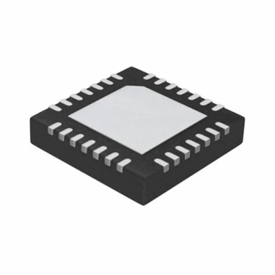
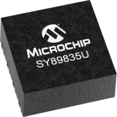
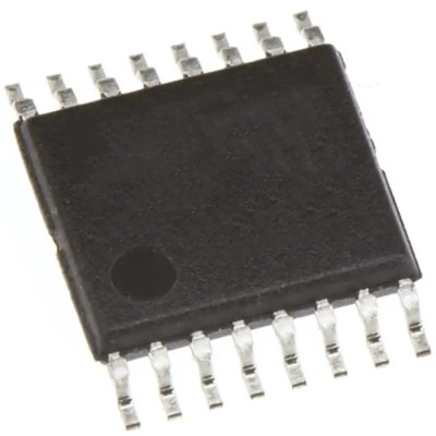
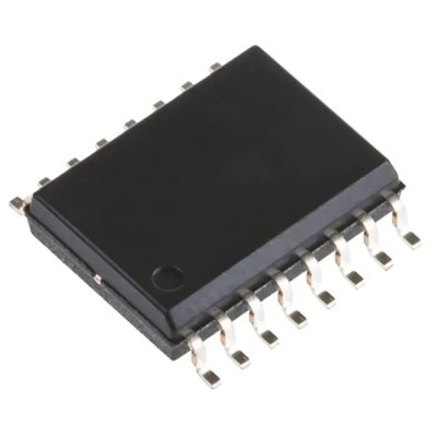
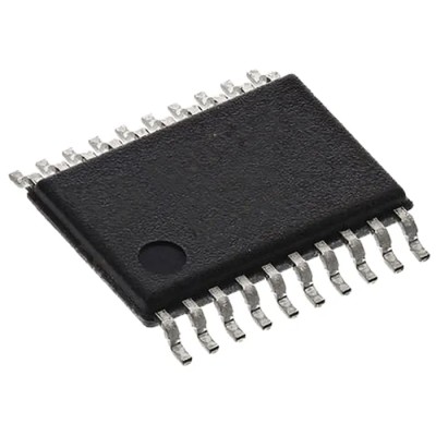
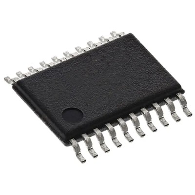
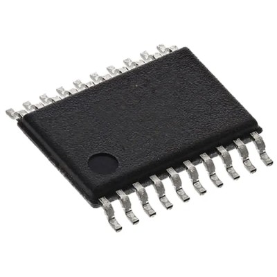
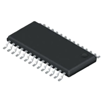
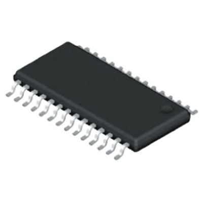
Renesas Electronics 9DB106BGLFT is a high-performance zero delay buffer designed specifically for clock timing applications, supporting PCIe Gen1 and Gen2 standards. This 28-pin TSSOP package buffer IC effectively attenuates jitter on the input clock signal, enhancing timing accuracy in complex electronic systems.
The device features selectable PLL bandwidth to minimize jitter peaking in downstream phase-locked loops (PLLs), adapting to systems with or without spread spectrum clocking. Its compatibility with spread spectrum input clocks helps reduce electromagnetic interference (EMI) in sensitive applications.
An integrated SMBus interface facilitates precise control over PLL bandwidth and allows unused outputs to be disabled, optimizing power efficiency. Additionally, two clock request pins make it suitable for ExpressCard applications, providing flexibility in modern computing environments.
Operated within a supply voltage window from 3.13V to 3.46V, the IC maintains reliable performance with a maximum input frequency of 105 MHz and a propagation delay time of 150 picoseconds. The surface-mount TSSOP package measuring 9.7 mm in length and 1 mm in height offers a compact form factor conducive to space-constrained PCB designs.
Designed for industrial and commercial use cases, this buffer IC supports clock management in electronic components, telecommunications equipment, and computing devices where low jitter and precise timing are critical.
Supports PCIe Gen1 and Gen2 clocking requirements. Selectable PLL bandwidth to optimize jitter performance. SMBus interface for bandwidth control and output disablement. Two clock request pins ideal for ExpressCard applications.
Operates between 3.13V and 3.46V supply voltage. Maximum input frequency of 105 MHz and 150 ps propagation delay. 28-pin TSSOP surface mount package with compact dimensions. Operational temperature range of 0°C to 70°C for reliable performance.
Compact dimensions: 9.7 mm length and 1 mm height.
This Renesas Electronics 9DB106BGLFT buffer is suitable for integration in semiconductor manufacturing, industrial electronics, computer hardware, and telecommunications equipment. It provides robust clock buffering functionality essential for maintaining signal integrity and timing accuracy in high-frequency digital systems.
Explore more clock buffer solutions and Renesas Electronics components in the EnvMart catalog to advance your design and system performance requirements.
Explore more products in our Clock Buffers category.




 Global Payments 140+ Countries
 Global Shipping Fedex/UPS/DHL/Aramex/
BlueDart/Delhivery/DP World
Global Shipping Fedex/UPS/DHL/Aramex/
BlueDart/Delhivery/DP World 24/7 Customer Support Email/Chat/Telephonic Support
Comments (0)
Your review appreciation cannot be sent
Report comment
Report sent
Your report cannot be sent