$4.90
$4.75
Tax included

World's First Climate Tech Platform | Free Delivery in India | Global Shipping

Shop with confidence knowing that our 24/7 Customer Support is always available to assist with any inquiries

Avail maximum benefits from input tax mechanism on all your Business Invoices. Get GST Invoices on your business purchases. And 0% Taxes on all worldwide deliveries

If you find this product anywhere at lower cost than us. Call us and we will not only match the price but also give a complimentary coupon

Shop with assurance, as each product we offer is 100% original, ensuring quality and authenticity with every purchase
| Country of Origin | India |
|---|---|
| Brand | Renesas Electronics |
| Height | 1mm |
| Length | 9.7mm |
| Model | 9DB106BGLFT |
| Mount Type | Surface |
| Series | 9DB106 |
| Maximum Operating Temperature | 70°C |
| Package Type | TSSOP |
| Minimum Operating Temperature | 0°C |
| Maximum input frequency | 105MHz |
| Standards/Approvals | PCIe Gen1 and Gen2 |
| Pin Count | 28 |
| Maximum Supply Voltage | 3.46V |
| Minimum Supply Voltage | 3.13V |
| Maximum Propagation Delay Time | 150ps |
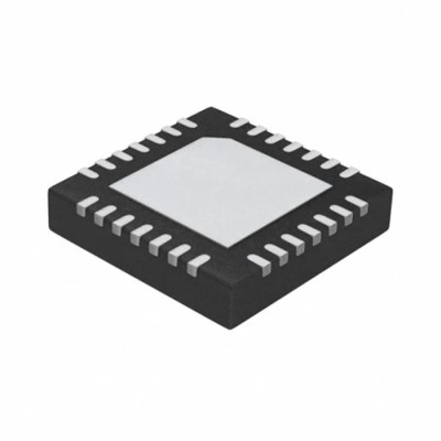
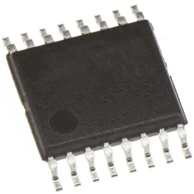
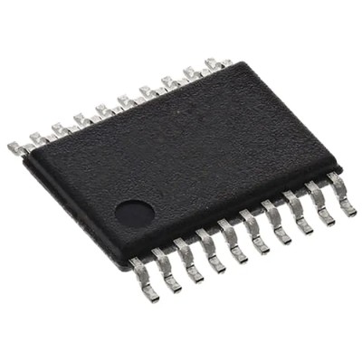
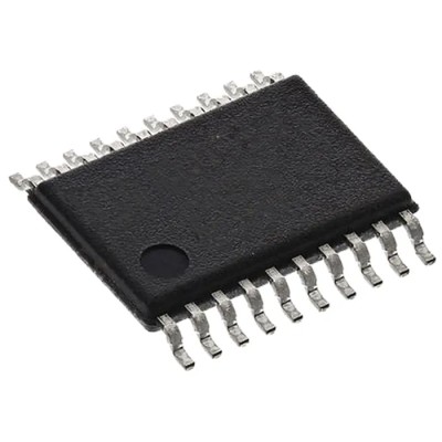
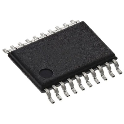
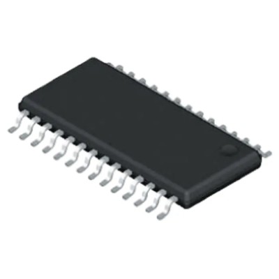
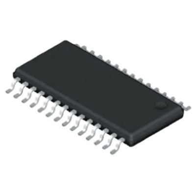
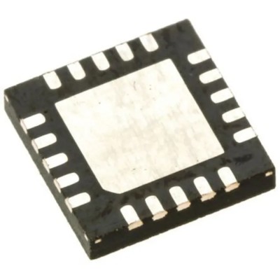
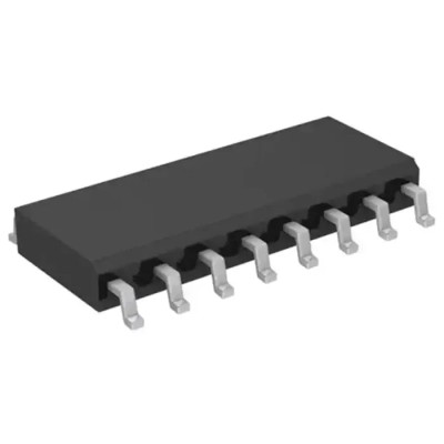
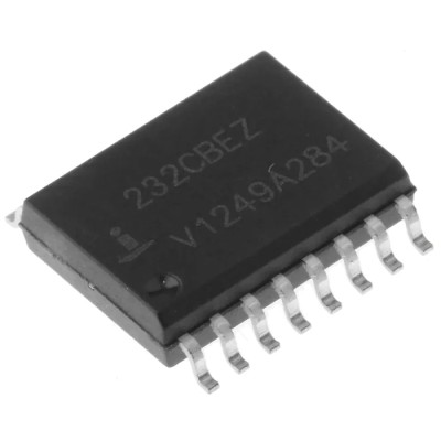
Renesas Electronics 9DB106BGLFT buffer 28-pin TSSOP is a high-performance clock buffer supporting PCIe Gen1 and Gen2 standards, designed to attenuate jitter and maintain signal integrity in advanced electronic systems. It receives a differential SRC output from an IDT-compliant main clock generator and offers selectable PLL bandwidth to adapt to system spread spectrum clocking.
The device incorporates an SMBus interface that allows the user to control PLL bandwidth and enable or disable unused outputs, facilitating flexible integration. Its two clock request pins enhance compatibility with Express Card standards, making it suitable for various embedded and computing applications.
Operating within a supply voltage range of 3.13V to 3.46V and temperature range of 0°C to 70°C, this buffer is surface-mounted in a compact 28-pin TSSOP package measuring 9.7mm in length and 1mm in height, enabling efficient board layout. It meets critical timing requirements with a maximum input frequency of 105MHz and low propagation delay time of 150ps, ensuring fast and reliable clock distribution.
This buffer is ideal for industrial, computing, telecommunications, and embedded system applications requiring low jitter and precise timing control. Its design emphasis on spread spectrum compatibility also reduces EMI in compliant systems.
This buffer attenuates jitter on input clocks for stable signal output. Selectable PLL bandwidth optimizes performance with or without spread spectrum clocking. Includes an SMBus interface for controlling PLL bandwidth and disabling unused outputs.
Features two clock request pins suitable for Express Card applications. Operates with supply voltage range from 3.13V to 3.46V. Mount type is surface mount with a compact 28-pin TSSOP package. Designed to operate reliably within 0°C to 70°C temperature range.
Physical dimensions include 9.7mm length and 1mm height for board space efficiency.
For professional designers and engineers, the Renesas Electronics 9DB106BGLFT buffer offers reliable, precise, and low-jitter clock buffering to meet modern high-performance system needs. Explore more semiconductor products at EnvMart to complement your design and manufacturing requirements.
Explore more products in our Clock Buffers category.
Review sent
Your review cannot be sent
Global Payments 140+ Countries
Global Shipping Fedex/UPS/DHL/Aramex/
BlueDart/Delhivery/DP World
24/7 Customer Support Email/Chat/Telephonic Support
Comments (0)
Your review appreciation cannot be sent
Report comment
Report sent
Your report cannot be sent