$2.28
$2.21
Tax included

World's First Climate Tech Platform | Free Delivery in India | Global Shipping

Shop with confidence knowing that our 24/7 Customer Support is always available to assist with any inquiries

Avail maximum benefits from input tax mechanism on all your Business Invoices. Get GST Invoices on your business purchases. And 0% Taxes on all worldwide deliveries

If you find this product anywhere at lower cost than us. Call us and we will not only match the price but also give a complimentary coupon

Shop with assurance, as each product we offer is 100% original, ensuring quality and authenticity with every purchase
| Country of Origin | India |
|---|---|
| Brand | Renesas Electronics |
| Height | 1mm |
| Length | 3.1mm |
| Model | 5PB1104PGGI8 |
| Mount Type | Surface |
| Series | 5PB |
| Maximum Operating Temperature | 105°C |
| Package Type | TSSOP |
| Minimum Operating Temperature | -40°C |
| Maximum input frequency | 200MHz |
| Pin Count | 8 |
| Maximum Supply Voltage | 3.3V |
| Minimum Supply Voltage | 1.8V |
| Maximum Propagation Delay Time | 250ps |
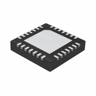
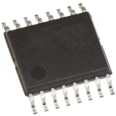
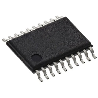
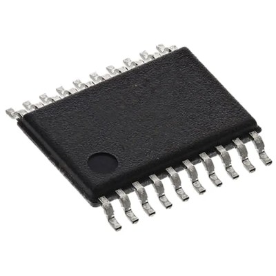
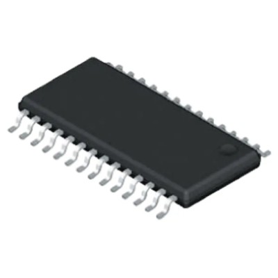
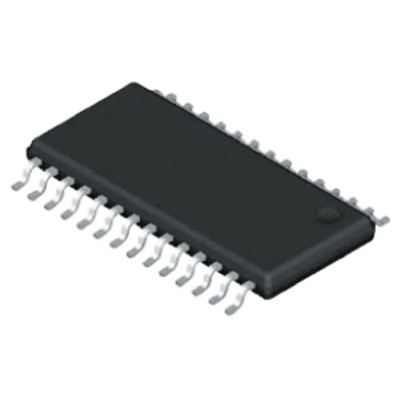
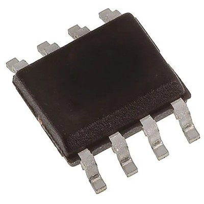
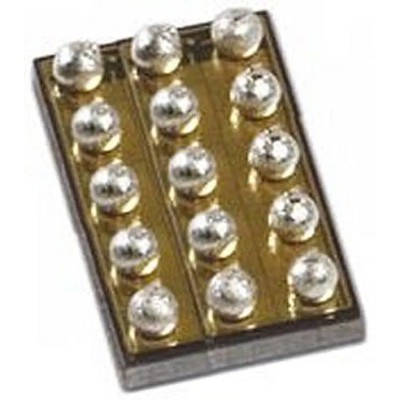
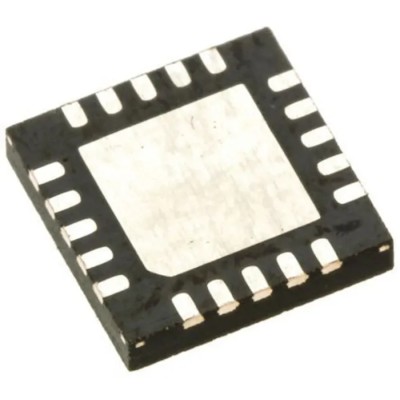
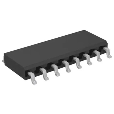
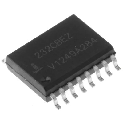
Renesas Electronics 5PB1104PGGI8 Clock Buffer is a high performance CMOS device in an 8-pin TSSOP package designed for surface mount applications. It features low additive phase jitter of 50fs RMS, ensuring signal integrity and timing precision in electronic systems.
This clock buffer supports input frequencies up to 200MHz and has a maximum propagation delay of just 250ps. Its operating voltage range spans from 1.8V to 3.3V, making it compatible with a variety of industrial and commercial electronic circuits.
Featuring very low pin-to-pin skew, this device helps minimize timing discrepancies among output signals. The integrated serial termination is optimized for 50 ohm channels, simplifying PCB design and signal conditioning. It also includes a synchronous glitch-free output enable function to prevent intermediate erroneous clock cycles during output enable or disable operations.
The clock buffer operates reliably over a wide temperature range from -40°C to 105°C, suitable for robust industrial, communication, automotive (though not automotive standard), and instrumentation applications. Its compact package measures 3.1mm in length and 1mm in height, fitting conveniently into space-constrained designs.
Supports 200MHz maximum input frequency. 250ps maximum propagation delay ensures fast timing response. Wide supply voltage range of 1.8V to 3.3V. Surface mount 8-pin TSSOP package. Operating temperature range -40°C to 105°C for durable performance.
Very low pin-to-pin skew for signal accuracy. Integrated 50 ohm serial termination optimizes signal integrity. Synchronous glitch-free output enable feature. Compact package dimensions (3.1mm × 1mm).
This 5PB1104PGGI8 clock buffer is suited for use in a broad range of electronic products requiring precise clock timing including industrial automation, telecommunications, networking, and electronic testing equipment.
Explore more products in the Clock Buffers category for additional solutions designed for timing and frequency control challenges.
Review sent
Your review cannot be sent
Global Payments 140+ Countries
Global Shipping Fedex/UPS/DHL/Aramex/
BlueDart/Delhivery/DP World
24/7 Customer Support Email/Chat/Telephonic Support
Comments (0)
Your review appreciation cannot be sent
Report comment
Report sent
Your report cannot be sent