$1.45
$1.40
Tax included

World's First Climate Tech Platform | Free Delivery in India | Global Shipping

Shop with confidence knowing that our 24/7 Customer Support is always available to assist with any inquiries

Avail maximum benefits from input tax mechanism on all your Business Invoices. Get GST Invoices on your business purchases. And 0% Taxes on all worldwide deliveries

If you find this product anywhere at lower cost than us. Call us and we will not only match the price but also give a complimentary coupon

Shop with assurance, as each product we offer is 100% original, ensuring quality and authenticity with every purchase
| Country of Origin | India |
|---|---|
| Brand | onsemi |
| Height | 900μm |
| Length | 12.5mm |
| Model | 74LCX16245MTDX |
| Mount Type | Surface |
| Output type | 3 State |
| Series | 74LCX16245 |
| Maximum Operating Temperature | 85°C |
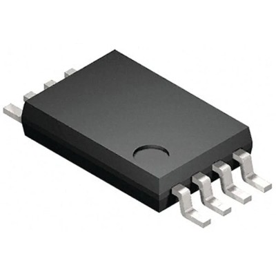
| Package Type | TSSOP |
| Minimum Operating Temperature | -40°C |
| Pin Count | 48 |
| Number of Elements per Chip | 1 |
| Maximum Supply Voltage | 3.6V |
| Logic Family | LCX |
| Logic Function | Buffer |
| Minimum Supply Voltage | 2V |
| Maximum High Level Output Current | -24mA |
| Maximum Propagation Delay Time @ CL | 5.4ns |
| Direction Type | Bi-Directional |
| Maximum Low Level Output Current | 24mA |
| Translation | Bi-Directional |
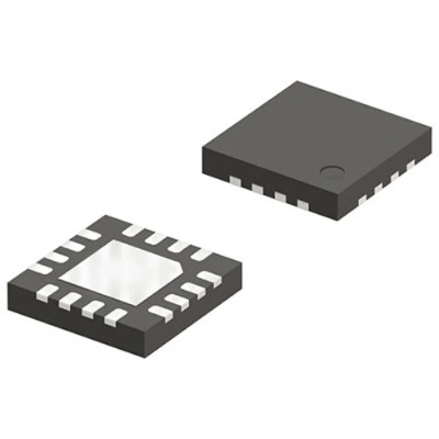
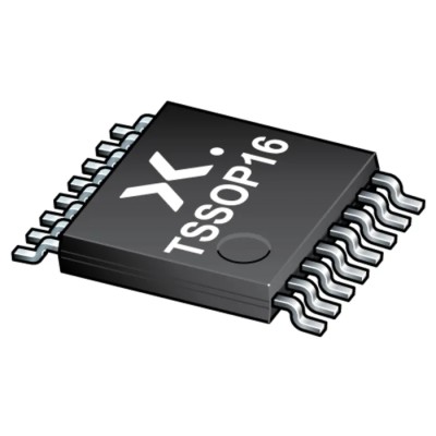
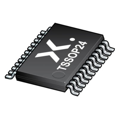
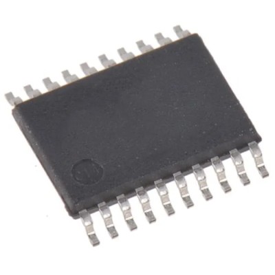
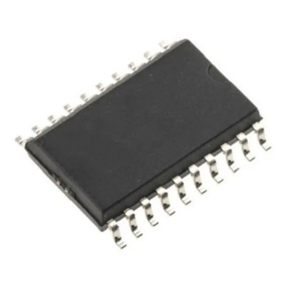
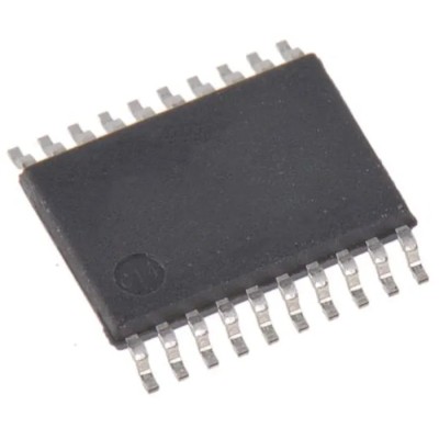
The onsemi 74LCX16245MTDX Voltage Level Shifter Buffer is a 48-pin TSSOP package logic IC specially designed to provide reliable bi-directional voltage level shifting with excellent signal integrity. Operating within a voltage range of 2.3V to 3.6V, this device supports a maximum propagation delay of 5.4 nanoseconds, ensuring fast digital logic response times in electronic applications.
Its 5V tolerant inputs and outputs make it suitable for interfacing with a variety of voltage domains, providing flexibility in mixed-voltage system designs. The buffer achieves high output drive strength of ±24 milliamps at 3.0V VCC, making it capable of driving larger capacitive loads without performance degradation.
Power down modes place inputs and outputs into high impedance states, enabling energy saving in complex or battery-operated systems. The IC features patented noise and electromagnetic interference (EMI) reduction technology, enhancing signal quality and device stability in industrial, communication, and consumer electronics.
Robust latch-up immunity exceeding 500 mA ensures device safety during unexpected electrical conditions. Electrostatic discharge (ESD) protection is designed for Human Body Model ratings greater than 2000 volts and Machine Model ratings greater than 200 volts, safeguarding against common static events encountered during handling and operation.
This component is ideally suited for use in industrial automation, data communication systems, consumer electronics, and embedded digital logic circuits requiring precise voltage level shifting and buffering.
Supports bi-directional voltage translation for broad compatibility. Features 5V tolerant inputs and outputs for flexible interfacing. Operating voltage range from 2.3V to 3.6V ensures low power consumption. Maximum propagation delay time of 5.4 ns provides fast signal processing.
High output drive capability with ±24 mA output drive at VCC = 3.0V. Power down high impedance inputs and outputs support system power saving. Designed with patented noise and EMI reduction circuitry for robustness. Latch-up performance exceeds 500 mA for enhanced reliability.
ESD protection compliant with Human Body Model > 2000V and Machine Model > 200V. Explore more semiconductor components and voltage translators in our Electronics & Electricals category at EnvMart.
Review sent
Your review cannot be sent
Global Payments 140+ Countries
Global Shipping Fedex/UPS/DHL/Aramex/
BlueDart/Delhivery/DP World
24/7 Customer Support Email/Chat/Telephonic Support
Comments (0)
Your review appreciation cannot be sent
Report comment
Report sent
Your report cannot be sent