$0.22
$0.21
Tax included

World's First Climate Tech Platform | Free Delivery in India | Global Shipping

Shop with confidence knowing that our 24/7 Customer Support is always available to assist with any inquiries

Avail maximum benefits from input tax mechanism on all your Business Invoices. Get GST Invoices on your business purchases. And 0% Taxes on all worldwide deliveries

If you find this product anywhere at lower cost than us. Call us and we will not only match the price but also give a complimentary coupon

Shop with assurance, as each product we offer is 100% original, ensuring quality and authenticity with every purchase
| Country of Origin | India |
|---|---|
| Brand | Toshiba |
| Height | 1mm |
| Length | 5mm |
| Model | 74VHC126FT |
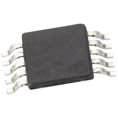
| Mount Type | Surface |
| Output type | 3 State |
| Series | 74VHC |
| Input Type | CMOS |
| Maximum Operating Temperature | 125°C |
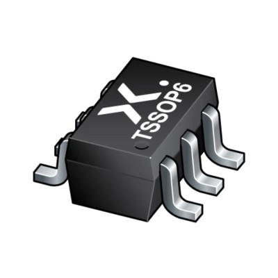
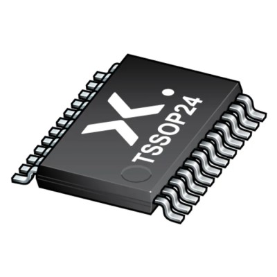
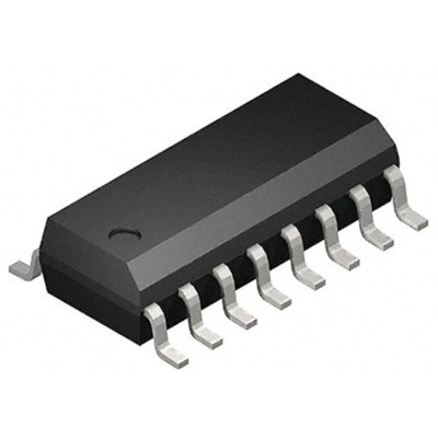
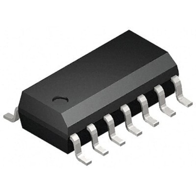
| Package Type | TSSOP |
| Minimum Operating Temperature | -40°C |
| Polarity | Non-Inverting |
| Pin Count | 14 |
| Automotive Standard | AEC-Q100 |
| Maximum Supply Voltage | 5.5V |
| Logic Family | 74VHC |
| Logic Function | Buffer |
| Minimum Supply Voltage | 2V |
| Maximum High Level Output Current | -8mA |
| Maximum Propagation Delay Time @ CL | 3.8ns |
| Supply Current | 4μA |
| Maximum Low Level Output Current | 8mA |
| Balanced propagation delays | tPLH ≈ tPHL |
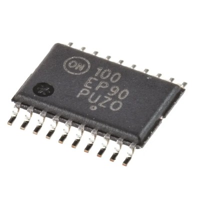
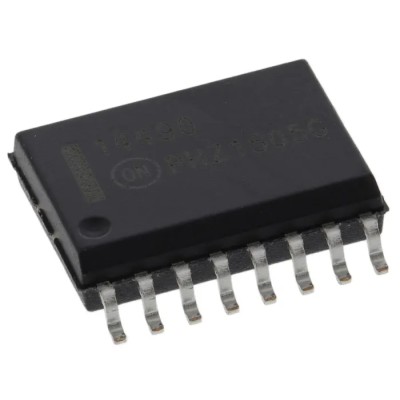
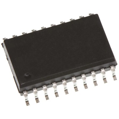
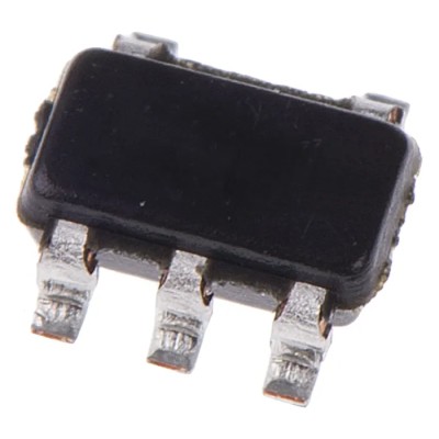
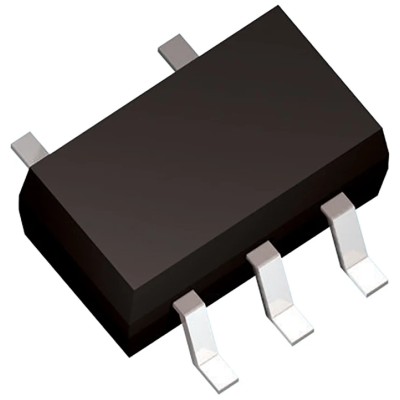
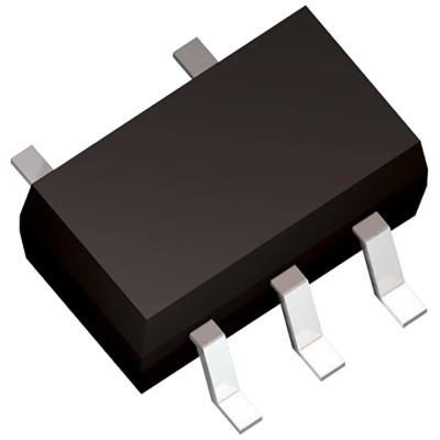
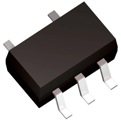
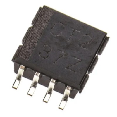
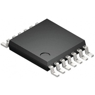
Toshiba 74VHC126FT is a Non-Inverting 3 State Octal Bus Buffer designed with silicon gate C2MOS technology for high-speed CMOS operation. This device combines the high-speed performance of Bipolar Schottky TTL with the low power consumption of CMOS technology, operating from 2 V to 5.5 V supply.
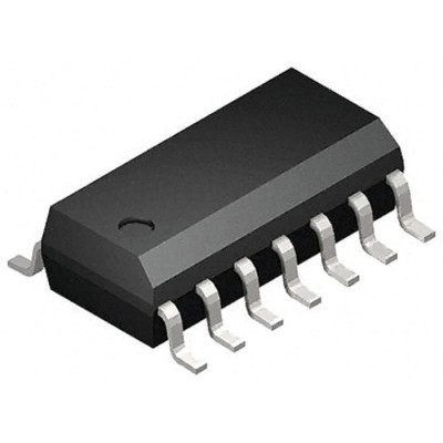
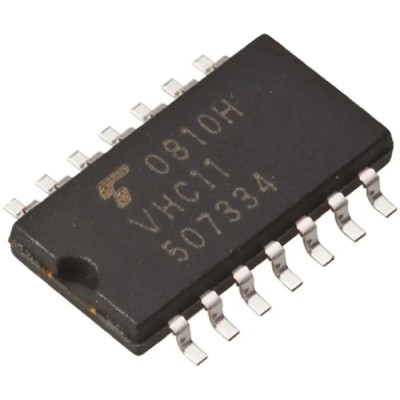
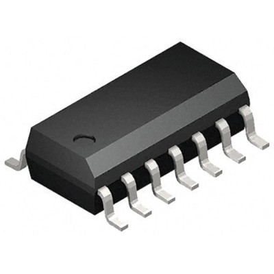
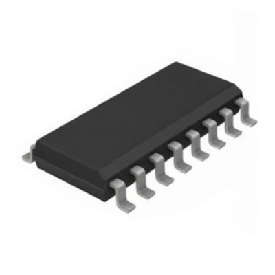
The 74VHC126FT features a 14-pin TSSOP surface mount package ideal for compact electronic circuit designs, providing low profile and space-saving benefits. With a typical propagation delay time of 3.8 ns at CL, it is suitable for applications demanding fast signal buffering and data bus driving capabilities.
The buffer operates as non-inverting with 3-state outputs controlled by input G (control input must be set low to enable high impedance output), allowing efficient bus interfacing and signal isolations.
Robust input protection circuitry permits the application of input voltages up to 5.5 V regardless of the supply voltage, enabling compatibility with mixed-voltage systems and battery-backed supplies.
The device supports a wide temperature operation range from -40°C to 125°C and meets the automotive AEC-Q100 standard, ensuring reliability in harsh environments.
The maximum output current is -8 mA for high-level and 8 mA for low-level output, with a low quiescent supply current of 4 μA at ambient 25°C, making it suitable for power-sensitive designs.
Operates from 2 V to 5.5 V supply voltage range. 14-pin TSSOP surface mount package. Typical propagation delay of 3.8 ns for high-speed operation. Non-inverting 3-state outputs suitable for bus buffering. Input protection allows voltages up to 5.5 V on input pins.
Wide temperature range of -40°C to 125°C. Meets automotive AEC-Q100 reliability standard. Low supply current of 4 μA at 25°C. Maximum high-level output current of -8 mA and low-level 8 mA.
This octal bus buffer is widely used in electronic circuits for buffer and line driver applications in consumer electronics, industrial control, automotive electronics, and communication systems.
Explore the extensive range of semiconductor components at EnvMart for high-quality industrial electronics and automation solutions.
Explore more products in our Logic ICs category.
Review sent
Your review cannot be sent
Global Payments 140+ Countries
Global Shipping Fedex/UPS/DHL/Aramex/
BlueDart/Delhivery/DP World
24/7 Customer Support Email/Chat/Telephonic Support
Comments (0)
Your review appreciation cannot be sent
Report comment
Report sent
Your report cannot be sent