$0.15
$0.14
Tax included

World's First Climate Tech Platform | Free Delivery in India | Global Shipping

Shop with confidence knowing that our 24/7 Customer Support is always available to assist with any inquiries

Avail maximum benefits from input tax mechanism on all your Business Invoices. Get GST Invoices on your business purchases. And 0% Taxes on all worldwide deliveries

If you find this product anywhere at lower cost than us. Call us and we will not only match the price but also give a complimentary coupon

Shop with assurance, as each product we offer is 100% original, ensuring quality and authenticity with every purchase
| Country of Origin | India |
|---|---|
| Brand | onsemi |
| Height | 550μm |
| Length | 1.25mm |
| Model | NTK3139PT1G |
| Width | 850μm |
| Mount Type | Surface |
| Series | NTK |
| Maximum Operating Temperature | 150°C |
| Package Type | SOT-723 |
| Minimum Operating Temperature | -55°C |
| Pin Count | 3 |
| Channel Type | Type P |
| Maximum Continuous Drain Current Id | 870mA |
| Maximum Drain Source Voltage Vds | 20V |
| Maximum Drain Source Resistance Rds | 2.2Ω |
| Channel Mode | Enhancement |
| Maximum Power Dissipation Pd | 550mW |
| Maximum Gate Source Voltage Vgs | -6, +6V |
| Forward Voltage Vf | -1.2V |
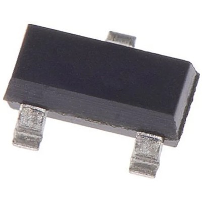
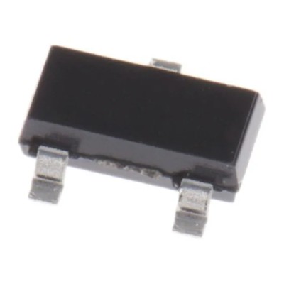
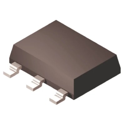
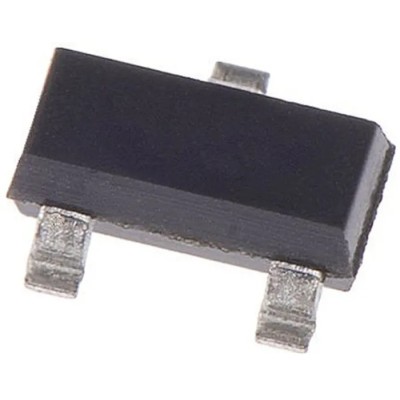
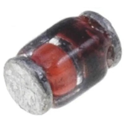
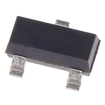
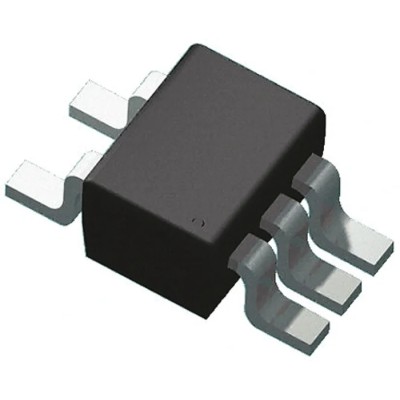
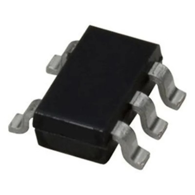
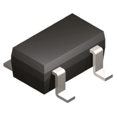
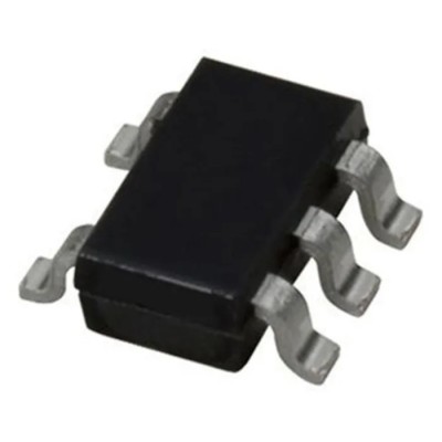
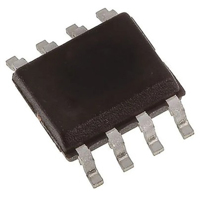
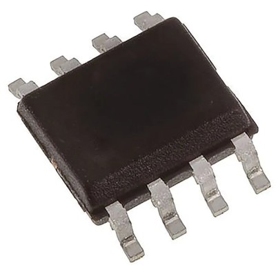
onsemi NTK3139PT1G is a P-Channel power MOSFET designed for surface mount technology packaged in the SOT-723 3-pin small outline transistor format. It offers maximum continuous drain current of 870 mA and supports a maximum drain-source voltage of 20V, making it ideal for low voltage switching applications.
This enhancement mode MOSFET features a maximum drain source resistance of 2.2 ohms, providing good conduction performance within compact device size constraints.
The device operates over a wide temperature range from -55°C up to 150°C, ensuring reliable operation in industrial, laboratory, and commercial electronic systems. Its forward voltage drop is relatively low at -1.2V, aiding energy efficiency in circuits.
Compact dimensions (length of 1.25 mm, width of 850 μm, and height of 550 μm) allow integration into high-density printed circuit boards, particularly for portable and space-restricted electronics.
The maximum gate-source voltage rating of -6 V to +6 V helps protect the transistor while maintaining high switching performance in both analog and digital power management designs.
Type P channel enhancement mode MOSFET designed for surface mount applications. Operates with maximum drain source resistance of 2.2 ohms. Encapsulated in compact SOT-723 package with 3 pins. Supports maximum gate-source voltage range of -6 to +6 volts.
Maximum power dissipation of 550mW ensuring efficient thermal handling. Wide operating temperature range from -55°C to 150°C for reliability in harsh environments. Dimensions: Length 1.25mm, Width 850µm, Height 550µm for space-sensitive circuits.
Suitable for applications requiring low forward voltage of -1.2V. Non-automotive standard MOSFET suitable for various industrial and electronic equipment uses.
This P-Channel MOSFET is widely used in power switching, load switching, and electronic control circuits across industrial and commercial electronics sectors. Its small size and moderate power capabilities also make it useful for laboratory and prototype development applications.
Explore more semiconductor and MOSFET products in the Electronics & Electricals category on EnvMart.
Explore more products in our Discrete Semiconductor category.
Review sent
Your review cannot be sent
Global Payments 140+ Countries

Global Shipping Fedex/UPS/DHL/Aramex/
BlueDart/Delhivery/DP World
24/7 Customer Support Email/Chat/Telephonic Support
Comments (0)
Your review appreciation cannot be sent
Report comment
Report sent
Your report cannot be sent