Vishay SI3993CDV-T1-GE3 is a P-Channel Power MOSFET from the TrenchFET series featuring an isolated transistor design. This component offers a maximum continuous drain current of 2.3 A, with a maximum drain-source voltage of 30 V, making it suitable for moderate current switching applications in compact electronic circuits.
The device employs enhancement mode operation, enabling easy implementation for high-side switching in battery-powered and DC load management systems. Its low on-resistance of 188 milliohms effectively reduces conduction losses, improving circuit efficiency and thermal performance.
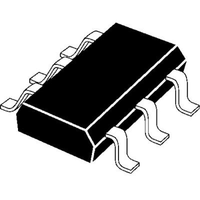
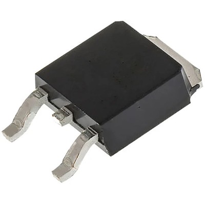
Encased in a 6-pin TSOP surface-mount package, the MOSFET supports compact PCB layouts and integrates two transistor elements, facilitating reliable power switching within space-constrained applications. The typical gate charge of 5.2 nC allows fast gate transitions, essential for efficient switching speeds.
Designed to operate within a wide temperature range from -55°C to +150°C, this MOSFET withstands severe thermal conditions found in industrial, consumer electronics, and automotive environments. The maximum power dissipation rating of 1.4 W further ensures effective thermal management in small form factors.
Common applications include battery-powered high-side switching circuits, DC load disconnects, reverse-current blocking, and power management modules within consumer electronic devices. The device accepts gate-source voltages up to ±20 V, requiring controlled gate drive circuitry to prevent gate stress.
Package dimensions are compact with a length of 3.1 mm, width of 1.7 mm, and height of 1 mm, facilitating integration into dense PCB assemblies. P-channel enhancement mode operation for high-side switching convenience. Maximum continuous drain current of 2.3 A supports moderate loads.
Low Rds(on) at 188 mΩ minimizes power loss during conduction. Typical gate charge of 5.2 nC enables rapid switching performance. Maximum power dissipation of 1.4 W supports thermal stability. 6-pin TSOP surface-mount package for compact PCB design.
Wide operational temperature range from -55°C to +150°C. Isolated transistor configuration with dual elements for reliable operation. Suitable for battery-powered, consumer, and power-management applications. Requires gate drive circuitry maintaining Vgs within ±20 V to avoid gate damage.
Explore Vishay and Power MOSFET categories on EnvMart for related components and advanced semiconductor solutions for your electronic design needs.



 Global Payments 140+ Countries
 Global Shipping Fedex/UPS/DHL/Aramex/
BlueDart/Delhivery/DP World
 24/7 Customer Support Email/Chat/Telephonic Support
Comments (0)
Your review appreciation cannot be sent
Report comment
Report sent
Your report cannot be sent