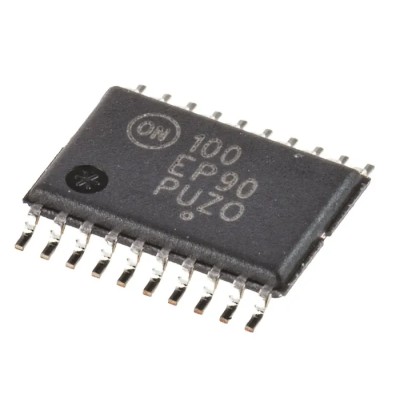
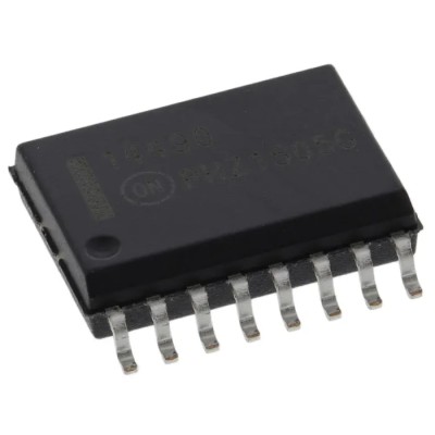
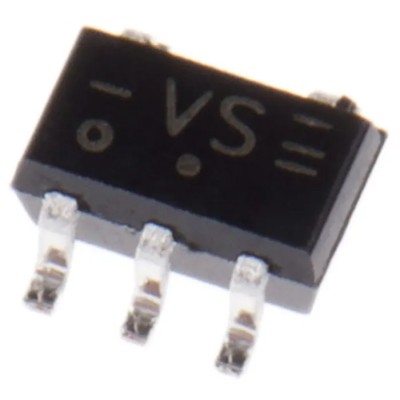
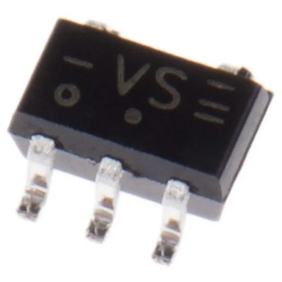
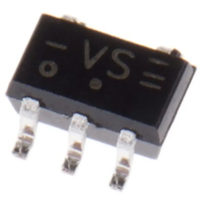
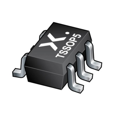
Nexperia 74HC595BZX is a precision 8-bit serial-in, serial or parallel-out surface mount shift register/latch logic IC designed for high-speed digital data conversion applications. It operates from a supply voltage range of 2 to 6 volts, making it versatile for various low-voltage industrial and electronic systems.
The device incorporates both a shift register and a storage register each clocked separately to allow flexible data manipulation in complex logic circuits. The asynchronous Master Reset (MR) input clears the shift register instantly, ensuring control over data flow in real-time applications.
Constructed with CMOS technology, the IC realizes low power dissipation and high noise immunity enhancing operational stability. Data bits are shifted on the rising edge of the Shift Clock (SHCP) input and latched into storage on the rising edge of the Storage Clock (STCP) input. This organization facilitates precise timing control in applications requiring synchronized data output.
Features include 3-state buffered outputs which can be disabled through the Output Enable (OE) pin, allowing multiple shift registers to share output lines safely in latch or bus architectures. The presence of clamp diodes on inputs enables interfacing with voltages exceeding VCC, broadening design flexibility.
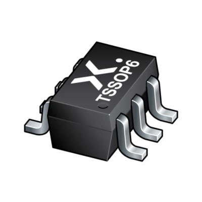
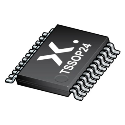
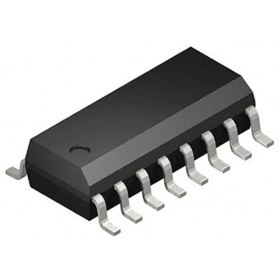
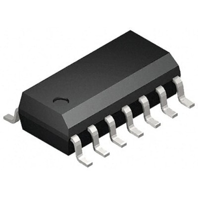
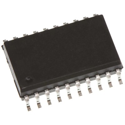
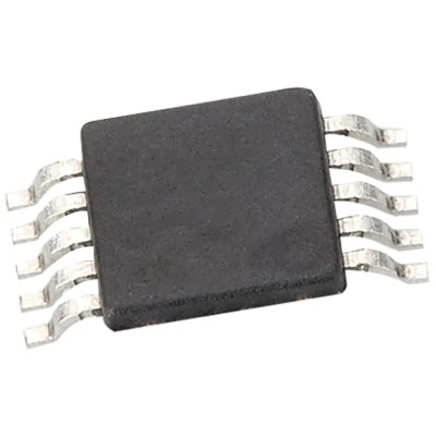
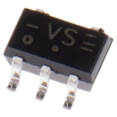
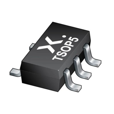
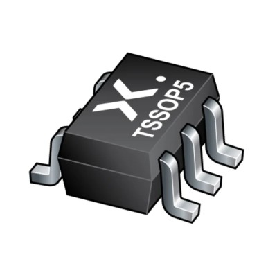
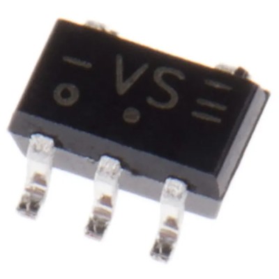
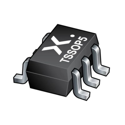
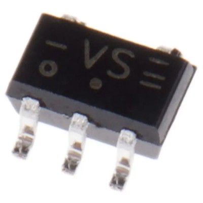
The 16-pin package measures 4.9mm by 4.3mm by 1.1mm, suitable for dense printed circuit board layouts and application in compact embedded systems. It complies with JEDEC and RoHS standards ensuring quality manufacturing and environmental safety.
Typical applications include industrial automation, data acquisition systems, embedded controllers, and digital signal processing where serial-to-parallel data conversion is essential for expanding microcontroller or FPGA output lines.
This device supports asynchronous master reset for immediate shift register clearing. Shift register and storage register use separate clocks enabling advanced timing control. Outputs have 3-state functionality facilitating safe data bus sharing.
CMOS construction ensures low power consumption and high noise immunity. Operating temperature rating up to 125°C suitable for industrial environments. Typical shift out frequency is 100 MHz, supporting high-speed digital circuits.
Complies with JEDEC and RoHS certifications. Compact 16-pin surface mount SO package dimensions optimize PCB space. Ideal for industrial, laboratory, embedded, and digital communication applications. Explore more advanced Logic ICs and Surface Mount Components at EnvMart to optimize your electronics assembly and manufacturing efficiency.



 Global Payments 140+ Countries
 Global Shipping Fedex/UPS/DHL/Aramex/
BlueDart/Delhivery/DP World
Global Shipping Fedex/UPS/DHL/Aramex/
BlueDart/Delhivery/DP World 24/7 Customer Support Email/Chat/Telephonic Support
Comments (0)
Your review appreciation cannot be sent
Report comment
Report sent
Your report cannot be sent