$0.54
$0.53
Tax included

World's First Climate Tech Platform | Free Delivery in India | Global Shipping

Shop with confidence knowing that our 24/7 Customer Support is always available to assist with any inquiries

Avail maximum benefits from input tax mechanism on all your Business Invoices. Get GST Invoices on your business purchases. And 0% Taxes on all worldwide deliveries

If you find this product anywhere at lower cost than us. Call us and we will not only match the price but also give a complimentary coupon

Shop with assurance, as each product we offer is 100% original, ensuring quality and authenticity with every purchase
| Country of Origin | India |
|---|---|
| Brand | Nexperia |
| Height | 850μm |
| Length | 2.4mm |
| Model | 74LVC2T45DC,125 |
| Mount Type | Surface |
| Compatibility | Input LVTTL/TTL, Output LVCMOS |
| Output type | 3 State |
| Input Type | Single Ended |
| Maximum Operating Temperature | 125°C |
| Package Type | VSSOP |
| Minimum Operating Temperature | -40°C |
| Polarity | Inverting |
| Number Of Channels | 4 |
| Operating Voltage | 1.65 to 5.5 V |
| Pin Count | 8 |
| Maximum Supply Voltage | 5.5V |
| Logic Family | LVC |
| Logic Function | Transceiver |
| Minimum Supply Voltage | 1.2V |
| Maximum High Level Output Current | -32mA |
| Maximum Propagation Delay Time @ CL | 15.2ns |
| Supply Current | 8μA |
| Maximum Low Level Output Current | 32mA |
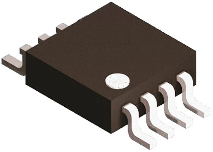
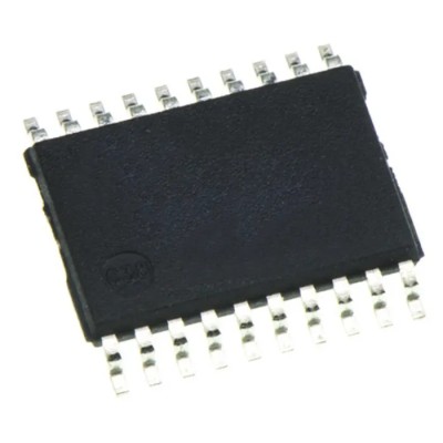
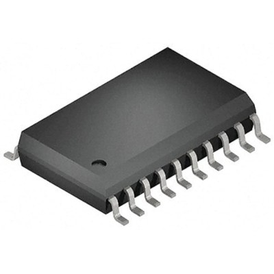
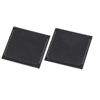
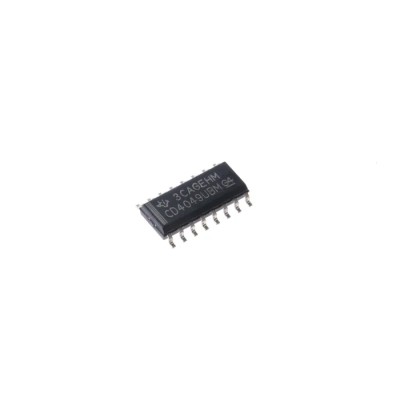
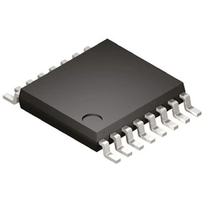
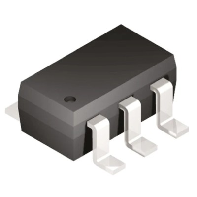
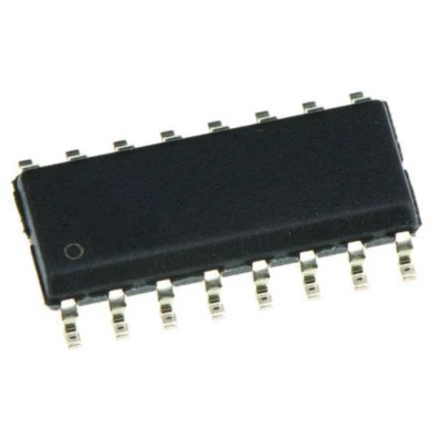
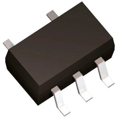
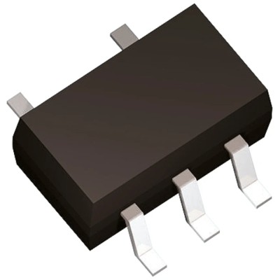
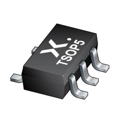
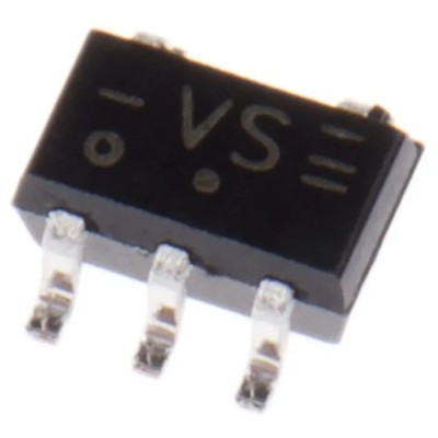
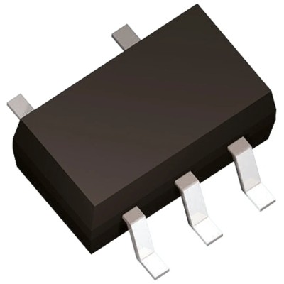
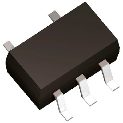
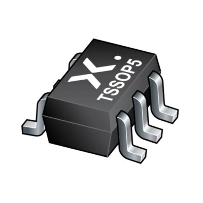
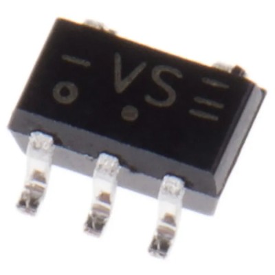
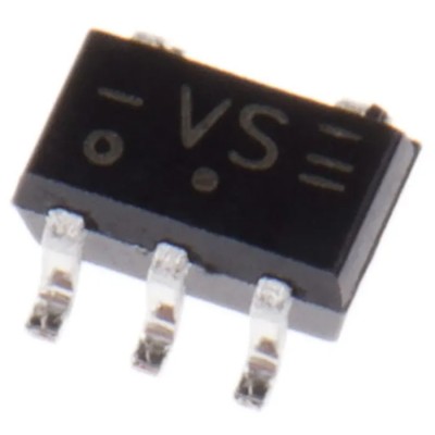
Nexperia 74LVC2T45DC,125 4-Channel Inverting 3 State Buffer & Converter Combination Circuit in an 8-pin VSSOP package is a low-voltage CMOS logic device tailored for efficient signal buffering and level shifting in electronic systems.
This device supports an operating voltage range from 1.65 V to 5.5 V, enabling versatile power supply schemes. It integrates four inverting channels with 3-state output capability, delivering precise digital signal inversion and tri-state buffer functionality.
With surface mount technology compatibility and compact packaging, it is designed for space-efficient PCB layouts. The buffer features maximum propagation delay of 15.2 ns at CL, ensuring fast signal transition suitable for timing-critical applications.
The product operates in a wide temperature range from -40°C to 125°C, making it reliable for industrial, automotive (non-automotive standard compliant), telecommunications, and general-purpose electronic applications.
The device draws a low supply current of 8 μA, improving overall power consumption in battery-powered or energy-conscious designs. Output currents can reach ±32 mA to drive various downstream circuit loads effectively.
Operates within a voltage range of 1.65 to 5.5 V allowing flexible power supply options. Includes four inverting channels with 3-state output functionality for efficient signal control. Designed for surface mount applications with a compact 8-pin VSSOP package.
Supports input levels compatible with LVTTL/TTL and outputs LVCMOS signals. Offers fast switching with a maximum propagation delay time of 15.2 ns at CL. Operates reliably in extreme temperatures from -40°C to 125°C suitable for diverse environments.
Features low supply current of 8 μA enhancing energy efficiency in circuits. Maximum output current up to ±32 mA accommodates various load requirements.
This buffer and converter combo circuit is ideal for industrial control systems, communication equipment, consumer electronics, and embedded system designs requiring robust signal interfacing and voltage level translation.
Explore a comprehensive selection of Buffers and digital ICs in the Electronics & Electricals category at EnvMart.
Review sent
Your review cannot be sent
Global Payments 140+ Countries

Global Shipping Fedex/UPS/DHL/Aramex/
BlueDart/Delhivery/DP World
24/7 Customer Support Email/Chat/Telephonic Support
Comments (0)
Your review appreciation cannot be sent
Report comment
Report sent
Your report cannot be sent