Previous
Next
Share
Free Delivery in India | Lowest Global Shipping Charges
24/7 Customer Support

Shop with confidence knowing that our 24/7 Customer Support is always available to assist with any inquiries

24/7 Customer Support
Save up to 28% with GST Input

Avail maximum benefits from input tax mechanism on all your Business Invoices. Get GST Invoices on your business purchases. And 0% Taxes on all worldwide deliveries

Lowest Price Challenge
# Lowest Price Challenge

If you find this product anywhere at lower cost than us. Call us and we will not only match the price but also give a complimentary coupon

Lowest Price Challenge
100% Original Products

Shop with assurance, as each product we offer is 100% original, ensuring quality and authenticity with every purchase

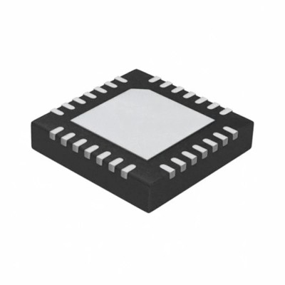
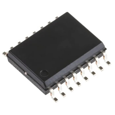
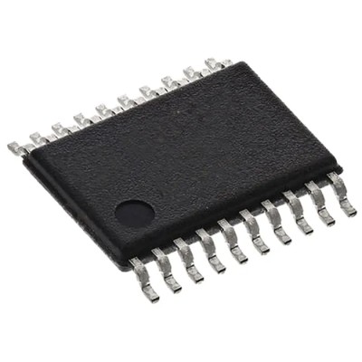
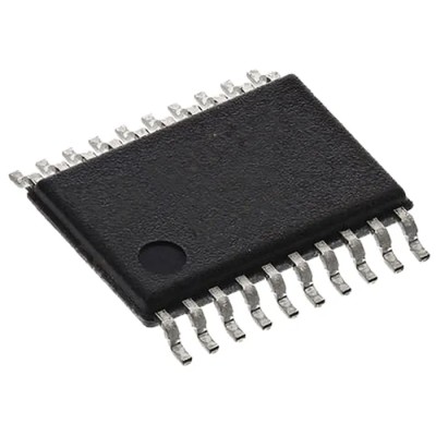
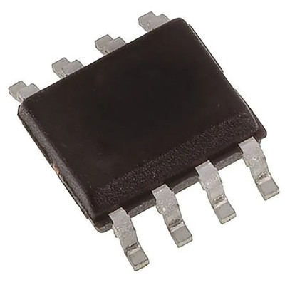
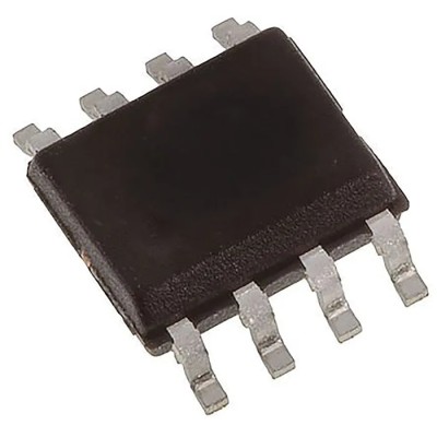
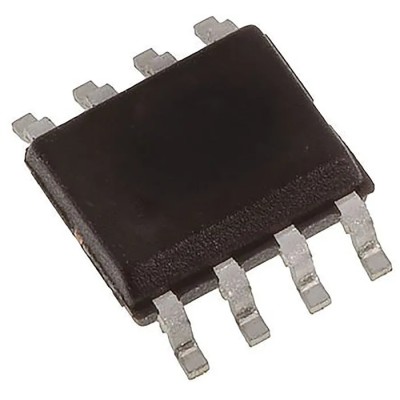
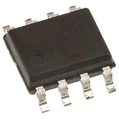
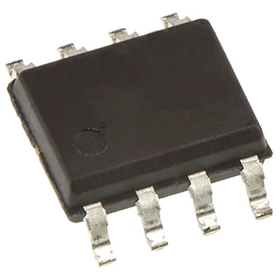
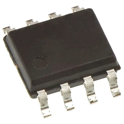
Infineon PLL Clock Buffer 8-Pin SOIC Voltage Range 3.3 V ± 5% or 5 V ± 10% CY2302SXI-1

Category Clock Buffers Brand Infineon Condition New

Specifications

Country of Origin India
Voltage Range 3.3 V ± 5%, or 5 V ± 10%
Brand Infineon
Height 1.47mm
Length 4.97mm
Model CY2302SXI-1
Maximum Operating Temperature 85°C
Package Type SOIC
Minimum Operating Temperature -40°C
Maximum input frequency 133MHz
Pin Count 8
Output frequency range 5 MHz to 133 MHz

Key Features

  • The device operates within a voltage range of 3.3 V ± 5% or 5 V ± 10%.
  • Supports output frequency from 5 MHz to 133 MHz.
  • Features two outputs with zero delay buffer and frequency multiplication capability.
  • Provides typical jitter performance of 91 ps on one output and 2200 ps on the other output.
  • Operates reliably from -40°C to 85°C ambient temperature range.
  • The 8-pin SOIC package measures 4.97 mm in length and 1.47 mm in height.
  • Offers configuration flexibility via an external feedback path for zero delay feature implementation.
  • Suitable for industrial, electronic component, and semiconductor applications that require clock synchronization.

Product Description

Infineon CY2302SXI-1 is a high-performance PLL clock buffer designed for precise timing and frequency management in electronic circuits. Packaged in an 8-pin SOIC, it supports an input clock frequency of up to 133 MHz and operates across a voltage range of 3.3 V ± 5% or 5 V ± 10%, ensuring versatile compatibility with diverse electronic systems.

The device integrates two buffered outputs providing zero delay functionality and frequency multiplication. Typical jitter values are 91 ps and 2200 ps on respective outputs, with an output-to-output skew of 165 ps and propagation delay around 90 ps. These timing characteristics enable stable clock distribution with minimal signal distortion.

Operating within a robust temperature range of -40°C to 85°C, this PLL clock buffer suits industrial and commercial semiconductor applications requiring reliable timing synchronization. Its compact SOIC package (length 4.97 mm, height 1.47 mm) facilitates easy PCB integration with minimal footprint.

Additional configuration options include an external feedback path, maximizing design flexibility to implement zero delay buffering tailored to system requirements. The device is ideal for clock distribution, synchronization, and frequency multiplication in telecommunications, computing, and industrial electronics.

Its low jitter and skew contribute to high signal integrity, essential for precision timing circuits. The wide voltage and temperature ranges ensure stable operation in varied operating environments. Compact 8-pin SOIC packaging aids in efficient space utilization and thermal management.

Infineon's CY2302SXI-1 PLL Clock Buffer is a reliable component for system designers needing precise clock timing with low jitter and flexible configuration capability. Explore more semiconductor Clock Buffers and related products at EnvMart for your electronic component requirements.

Infineon PLL Clock Buffer 8-Pin SOIC Voltage Range 3.3 V ± 5% or 5 V ± 10% CY2302SXI-1
Looking to purchase in bulk?
  • Purchase item in bulk quantity
  • Get best price for your business

Comments (0)

No customer reviews for the moment.

Frequently Asked Questions

This model operates within a voltage range of 3.3 V ± 5% or 5 V ± 10%.

The maximum input frequency supported by the CY2302SXI-1 is 133 MHz.

It supports an output frequency range from 5 MHz to 133 MHz.

The typical jitter performance is 91 ps on one output and 2200 ps on the other output.

This model operates reliably within an ambient temperature range of -40°C to 85°C.

The package measures 4.97 mm in length and 1.47 mm in height.

Yes, it features two outputs with zero delay buffer functionality.

The output-to-output skew is 165 ps.

It is suitable for industrial, electronic component, and semiconductor applications that require clock synchronization.

Key features include frequency multiplication capability, external feedback path for configuration flexibility, and low jitter performance.

The CY2302SXI-1 has a pin count of 8.

The country of origin for the CY2302SXI-1 is India.

Related Products

Other Products from this brand

$11.46
$11.12 Save 3%
Tax included
Quantity
Delivery Time Delivered within 0-3 days
  • Global Payments 140+ CountriesGlobal Payments 140+ Countries
  • Global Shipping Fedex/UPS/DHL/Aramex/
BlueDart/Delhivery/DP WorldGlobal Shipping Fedex/UPS/DHL/Aramex/ BlueDart/Delhivery/DP World
  • 24/7 Customer Support Email/Chat/Telephonic Support24/7 Customer Support Email/Chat/Telephonic Support
$11.46
$11.12
Tax included