$0.95
$0.93
Tax included

World's First Climate Tech Platform | Free Delivery in India | Global Shipping

Shop with confidence knowing that our 24/7 Customer Support is always available to assist with any inquiries

Avail maximum benefits from input tax mechanism on all your Business Invoices. Get GST Invoices on your business purchases. And 0% Taxes on all worldwide deliveries

If you find this product anywhere at lower cost than us. Call us and we will not only match the price but also give a complimentary coupon

Shop with assurance, as each product we offer is 100% original, ensuring quality and authenticity with every purchase
| Country of Origin | India |
|---|---|
| Brand | Renesas Electronics |
| Height | 1.75mm |
| Length | 5mm |
| Model | 2305-1DCG |
| Mount Type | Surface |
| Series | 2305-1DCG |
| Maximum Operating Temperature | 70°C |
| Package Type | SOIC |
| Minimum Operating Temperature | 0°C |
| Maximum input frequency | 133MHz |
| Pin Count | 8 |
| Maximum Supply Voltage | 3.6V |
| Minimum Supply Voltage | 3V |
| Maximum Propagation Delay Time | 250ps |
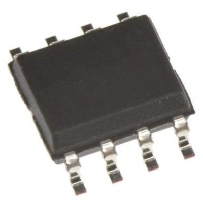
Renesas Electronics 2305-1DCG is a low phase noise, high-speed PLL based clock buffer in an 8-pin SOIC package designed for advanced clock timing applications.
This clock buffer supports a maximum input frequency of 133 MHz and achieves a maximum propagation delay of 250 picoseconds, enabling precise timing synchronization in electronic systems.
It uses Renesas' proprietary PLL technology developed from IDT techniques to provide four low skew outputs, making it suitable for demanding low jitter and zero delay applications.
The device operates over a voltage supply range of 3 V to 3.6 V and an ambient temperature range of 0°C to 70°C, supporting stable operation under typical industrial conditions.
The 2305-1DCG offers versatile output configurations including PLL sourced outputs for zero delay, direct input routed outputs for testing, and tri-state or low output states for control flexibility.
This product is intended for use in electronics, industrial communication, computing, and embedded system applications where accurate clock distribution is critical. The device supports a maximum input frequency of 133 MHz.
Maximum propagation delay time is 250 picoseconds. Features four low skew clock outputs with low jitter. Operates on a supply voltage range of 3 V to 3.6 V. Package type is an 8-pin Small Outline Integrated Circuit (SOIC).
Operating temperature range from 0°C to 70°C for industrial use cases. PLL feedback is integrated on-chip, ensuring zero input-output delay. Outputs can be set to tri-state mode or stopped at low level for signal control.
Compact dimensions of length 5 mm and height 1.75 mm allow space-efficient PCB layout.
Industrial electronic systems such as telecommunications equipment, data converters, and computing devices can benefit from this device by enhancing clock timing reliability and reducing signal skew.
Explore the Electronics & Electricals category on EnvMart for advanced semiconductor components including Clock Buffers by Renesas Electronics and other leading manufacturers.
Review sent
Your review cannot be sent
Global Payments 140+ Countries

Global Shipping Fedex/UPS/DHL/Aramex/
BlueDart/Delhivery/DP World
24/7 Customer Support Email/Chat/Telephonic Support
Comments (0)
Your review appreciation cannot be sent
Report comment
Report sent
Your report cannot be sent