Previous
Next
Share
Free Delivery in India | Lowest Global Shipping Charges
24/7 Customer Support

Shop with confidence knowing that our 24/7 Customer Support is always available to assist with any inquiries

24/7 Customer Support
Save up to 28% with GST Input

Avail maximum benefits from input tax mechanism on all your Business Invoices. Get GST Invoices on your business purchases. And 0% Taxes on all worldwide deliveries

Lowest Price Challenge
# Lowest Price Challenge

If you find this product anywhere at lower cost than us. Call us and we will not only match the price but also give a complimentary coupon

Lowest Price Challenge
100% Original Products

Shop with assurance, as each product we offer is 100% original, ensuring quality and authenticity with every purchase

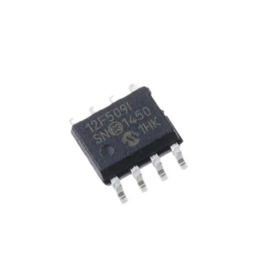
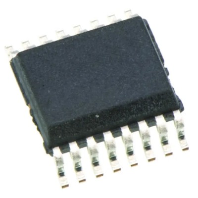
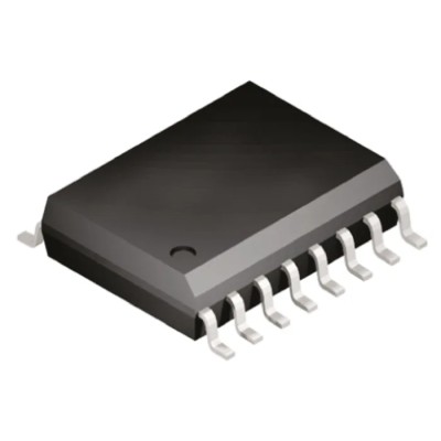
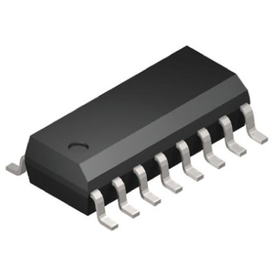
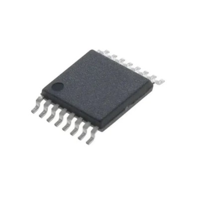
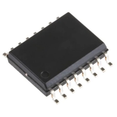
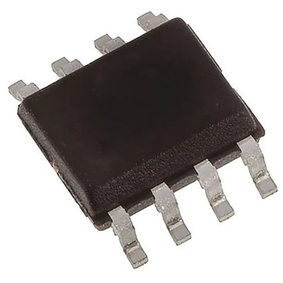
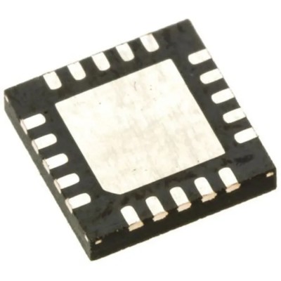
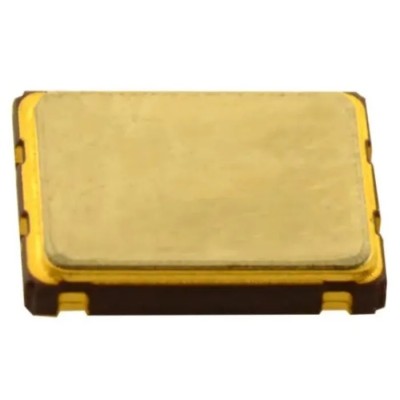
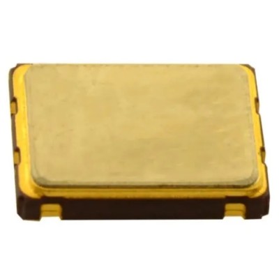
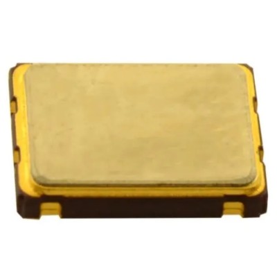
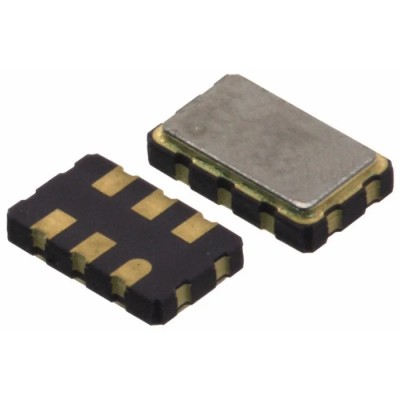
Renesas Electronics LVDS Buffer 2 TTL Buffer 20-Pin TSSOP 3-3.3V Operating -40°C to 85°C 9DB102BGILF

Category Electronic Components Brand Renesas Electronics Condition New

Specifications

Country of Origin India
Brand Renesas Electronics
Height 1.05mm
Length 6.6mm
Model 9DB102BGILF
Mount Type Surface
Output type Buffer
Series 9DB102
Input Type TTL
Maximum Operating Temperature 85°C
Package Type TSSOP
Sub Type Buffer
Minimum Operating Temperature -40°C
Pin Count 20
Number of Elements per Chip 2
Maximum Supply Voltage 3.3V
Minimum Supply Voltage 3V
Number of Drivers 2

Key Features

  • The device features 2 drivers and 2 elements per chip for efficient signal buffering.
  • It accepts TTL input type and provides buffered LVDS output signals.
  • Surface mount package type TSSOP ensures easy PCB integration.
  • Compact dimensions with 6.6mm length and 1.05mm height guarantee space-saving design.
  • Enhanced with ESD protection for robust industrial usage and reliability.
  • Supports zero delay buffer mode and fanout mode optimizing PCI Express clocking requirements.
  • Programmable bandwidth with operation frequency ranges of 33-110 MHz in PLL mode and 10-110 MHz in bypass mode.
  • Designed to minimize jitter, achieving phase jitter below 3.1 ps rms at PCIe Gen2.

Product Description

Renesas Electronics 9DB102BGILF is a 2-driver LVDS buffer with TTL input, available in a 20-pin TSSOP surface mount package. It operates with supply voltages from 3V to 3.3V and supports a wide temperature range from -40°C to 85°C, making it suitable for industrial and electronic component applications.

The device provides zero delay buffer and fanout modes, optimizing clock jitter mitigation for PCI Express systems. Featuring two 0.7 V HCSL differential output pairs, it offers phase jitter performance of less than 3.1 ps rms for PCIe Gen2 and under 86 ps peak-to-peak for PCIe Gen1. Bandwidth is programmable, with a range of 33 to 110 MHz in PLL mode and 10 to 110 MHz in bypass mode.

This LVDS interface IC supports jitter attenuation and compatible operation with differential SRC output pairs from IDT CK409/CK410-compliant main clock generators such as Renesas 952601 or 954101. Its compact 6.6mm by 1.05mm dimensions and ESD protection ensure durability and integration ease.

Commonly used in industrial, laboratory, communications, and high-speed digital equipment, the 9DB102BGILF buffer ensures precise timing control and reliable signal distribution in complex electronic systems.

The buffer IC is designed for PCI Express clocking and other high-speed serial data applications. Programmable PLL bandwidth adjusts for systems both with and without spread spectrum clocking. Compact 20-pin TSSOP package eases PCB layout and efficient placement.

Wide operating temperature range suitable for harsh environments. Integration with standard clock generators supports straightforward system design.

Explore the broad range of semiconductor components for electronics system design at EnvMart. Discover trusted brands and advanced ICs engineered to meet precise industrial applications.

Explore more products in our Electronic Components category.

Renesas Electronics LVDS Buffer 2 TTL Buffer 20-Pin TSSOP 3-3.3V Operating -40°C to 85°C 9DB102BGILF
Looking to purchase in bulk?
  • Purchase item in bulk quantity
  • Get best price for your business

Comments (0)

No customer reviews for the moment.

Frequently Asked Questions

This model operates within a temperature range of -40°C to 85°C, making it suitable for various industrial applications.

It requires a supply voltage between 3V and 3.3V for proper operation.

This unit features two drivers, allowing for efficient signal buffering.

It accepts TTL input type, which is standard for many electronic components.

The device has compact dimensions of 6.6mm in length and 1.05mm in height, facilitating easy PCB integration.

It achieves phase jitter performance of less than 3.1 ps rms for PCIe Gen2 and under 86 ps peak-to-peak for PCIe Gen1.

This buffer is available in a 20-pin TSSOP surface mount package, which simplifies installation on PCBs.

It supports zero delay buffer mode and fanout mode, optimizing clock jitter mitigation for PCI Express systems.

The bandwidth is programmable, ranging from 33 to 110 MHz in PLL mode and 10 to 110 MHz in bypass mode.

It is commonly used in industrial, laboratory, communications, and high-speed digital equipment applications.

Yes, it is enhanced with ESD protection, ensuring reliability in industrial usage.

This model contains two elements per chip, contributing to its efficient signal buffering capabilities.

Related Products

Other Products from this brand

$4.66
$4.52 Save 3%
Tax included
Quantity
Delivery Time Delivered within 0-3 days
  • Global Payments 140+ CountriesGlobal Payments 140+ Countries
  • Global Shipping Fedex/UPS/DHL/Aramex/
BlueDart/Delhivery/DP WorldGlobal Shipping Fedex/UPS/DHL/Aramex/ BlueDart/Delhivery/DP World
  • 24/7 Customer Support Email/Chat/Telephonic Support24/7 Customer Support Email/Chat/Telephonic Support
$4.66
$4.52
Tax included