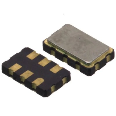
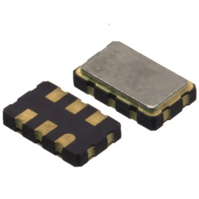
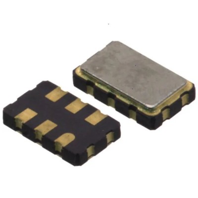
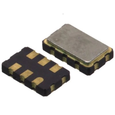
Previous
Next
Share
Free Delivery in India | Lowest Global Shipping Charges
24/7 Customer Support

Shop with confidence knowing that our 24/7 Customer Support is always available to assist with any inquiries

24/7 Customer Support
Save up to 28% with GST Input

Avail maximum benefits from input tax mechanism on all your Business Invoices. Get GST Invoices on your business purchases. And 0% Taxes on all worldwide deliveries

Lowest Price Challenge
# Lowest Price Challenge

If you find this product anywhere at lower cost than us. Call us and we will not only match the price but also give a complimentary coupon

Lowest Price Challenge
100% Original Products

Shop with assurance, as each product we offer is 100% original, ensuring quality and authenticity with every purchase

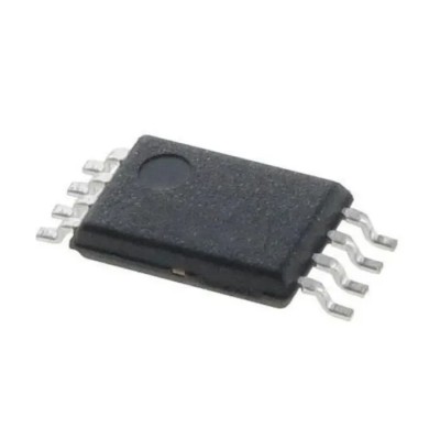
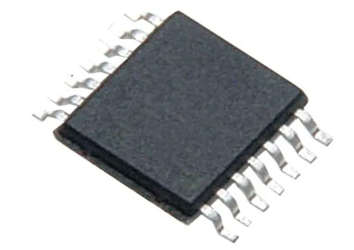
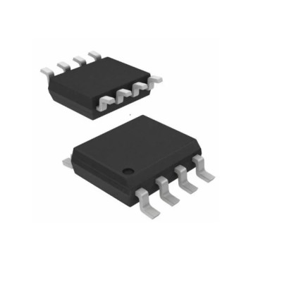
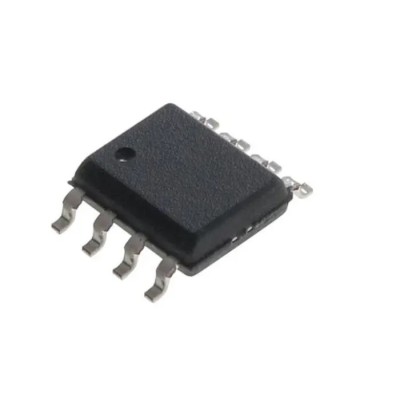
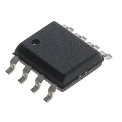
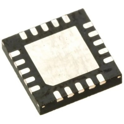
Renesas Electronics High-Performance LVCMOS Clock Buffer 14-Pin TSSOP 1.8V to 3.3V 200MHz 5PB1106PGGI

Category Clock Buffer Brand Renesas Electronics Condition New

Specifications

Country of Origin India
Brand Renesas Electronics
Height 1mm
Length 5mm
Model 5PB1106PGGI
Mount Type Surface
Series 5PB1106
Maximum Operating Temperature 105°C
Package Type TSSOP
Minimum Operating Temperature -40°C
Supply Voltage 1.8V to 3.3V
Maximum Output Frequency 200MHz
Pin Count 14
Maximum Supply Voltage 3.3V
Minimum Supply Voltage 1.8V

Key Features

  • High-performance LVCMOS clock buffer family with additive phase jitter of 50fs RMS.
  • Synchronous glitch-free output enable function prevents spurious clocks.
  • Operates within temperature range from -40°C to 105°C for robust industrial use.
  • Includes integrated serial termination for 50Ω channel to enhance signal quality.
  • Very low pin-to-pin skew of less than 50ps for precise timing applications.
  • 3.3V tolerant input clock supports compatibility with different logic levels.
  • Compact 14-pin TSSOP package with length 5mm and height 1mm for PCB space efficiency.
  • Suitable for industrial, automotive, and telecommunications applications requiring accurate clock distribution.

Product Description

The Renesas Electronics 5PB1106PGGI is a high-performance LVCMOS clock buffer designed in a 14-pin TSSOP package. It supports a supply voltage range from 1.8V to 3.3V and delivers a maximum output frequency of 200MHz, making it highly suitable for precision clock distribution purposes in electronic applications.

This device family features very low additive jitter below 50 femtoseconds RMS and offers fan-out options ranging from 1:2 up to 1:10. Its synchronous glitch-free output enable (OE) function ensures no intermediate erroneous clocks during output transitions, critical for timing-sensitive systems.

Operating within a wide temperature range from -40°C to 105°C, the 5PB1106PGGI is reliable for demanding industrial environments. Its 3.3V tolerant input clock and integrated serial 50Ω termination help maintain signal integrity and compatibility with various logic families.

The compact dimensions of 5mm length and 1mm height in the TSSOP package minimize PCB footprint while maximizing performance. This clock buffer is ideal for applications in industrial controls, automotive electronics, telecommunications infrastructure, and general-purpose timing circuits.

High-performance LVCMOS Clock Buffer family with additive phase jitter of 50fs RMS. Fan-out variations from 1:2 to 1:10 available for flexible clock distribution. Synchronous glitch-free output enable function prevents spurious clocks.

Wide operating temperature from -40°C to 105°C supports rugged environments. Integrated 50Ω serial termination enhances signal quality and reduces reflections. Very low pin-to-pin skew below 50ps ensures timing precision across outputs.

3.3V tolerant input clock for broad compatibility. Compact 14-pin TSSOP package with small form factor for PCB efficiency. Suitable for industrial, automotive, and telecommunications use cases. Explore the extensive Renesas Electronics portfolio in clock drivers and distribution devices at EnvMart for reliable semiconductor components tailored to your engineering needs.

Renesas Electronics High-Performance LVCMOS Clock Buffer 14-Pin TSSOP 1.8V to 3.3V 200MHz 5PB1106PGGI
Looking to purchase in bulk?
  • Purchase item in bulk quantity
  • Get best price for your business

Comments (0)

No customer reviews for the moment.

Frequently Asked Questions

The maximum output frequency of the 5PB1106PGGI clock buffer is 200MHz.

This clock buffer operates within a supply voltage range of 1.8V to 3.3V.

The operating temperature range for this model is from -40°C to 105°C.

This clock buffer has a total of 14 pins.

The 5PB1106PGGI is packaged in a 14-pin TSSOP format.

The pin-to-pin skew for the 5PB1106PGGI is less than 50ps.

Yes, it includes a synchronous glitch-free output enable function that prevents spurious clocks during transitions.

This model includes integrated serial 50Ω termination to enhance signal quality.

The 5PB1106PGGI is suitable for applications in industrial controls, automotive electronics, and telecommunications infrastructure.

The additive phase jitter for the 5PB1106PGGI is 50 femtoseconds RMS.

The fan-out options for this model range from 1:2 up to 1:10.

The TSSOP package has a height of 1mm and a length of 5mm.

Related Products

Other Products from this brand

Recently Viewed Products

$3.15
$3.06 Save 3%
Tax included
Quantity
Delivery Time Delivered within 0-3 days
  • Global Payments 140+ CountriesGlobal Payments 140+ Countries
  • Global Shipping Fedex/UPS/DHL/Aramex/
BlueDart/Delhivery/DP WorldGlobal Shipping Fedex/UPS/DHL/Aramex/ BlueDart/Delhivery/DP World
  • 24/7 Customer Support Email/Chat/Telephonic Support24/7 Customer Support Email/Chat/Telephonic Support
$3.15
$3.06
Tax included