$10.46
$10.14
Tax included

World's First Climate Tech Platform | Free Delivery in India | Global Shipping

Shop with confidence knowing that our 24/7 Customer Support is always available to assist with any inquiries

Avail maximum benefits from input tax mechanism on all your Business Invoices. Get GST Invoices on your business purchases. And 0% Taxes on all worldwide deliveries

If you find this product anywhere at lower cost than us. Call us and we will not only match the price but also give a complimentary coupon

Shop with assurance, as each product we offer is 100% original, ensuring quality and authenticity with every purchase
| Country of Origin | India |
|---|---|
| Brand | Renesas Electronics |
| Height | 1mm |
| Length | 4.9mm |
| Model | 83026BMI-01LF |
| Mount Type | Surface |
| Series | 83026BMI-01 |
| Maximum Operating Temperature | 85°C |
| Package Type | SOIC |
| Minimum Operating Temperature | -40°C |
| Maximum Output Frequency | 350MHz |
| Pin Count | 8 |
| Maximum Supply Voltage | 3.3V |
| Minimum Supply Voltage | 3V |
| Output skew | 15ps (maximum) |
| Part-to-part skew | 600ps (maximum) |
| Input levels | LVPECL, LVDS, LVHSTL, HCSL, SSTL |
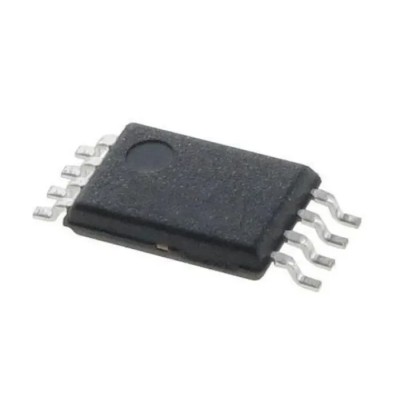
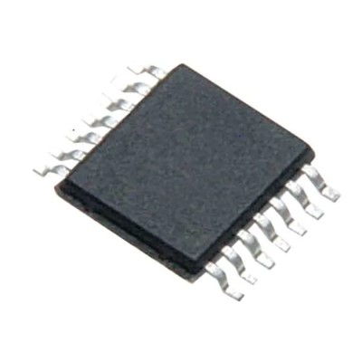
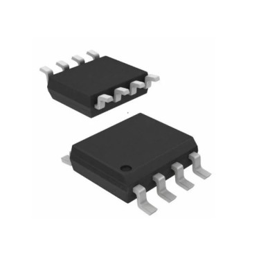
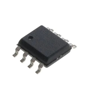
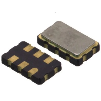
Renesas Electronics 83026BMI-01LF is a high-performance clock buffer designed for precision timing in electronic systems. It features a low skew 1-to-2 differential-to-LVCMOS/LVTTL fanout buffer functionality capable of accepting a wide range of differential input signal types, including LVPECL, LVDS, LVHSTL, HCSL, and SSTL. This versatility makes it ideal for applications needing reliable clock distribution with minimal signal distortion and jitter.
The device supports a maximum output frequency of 350MHz, providing two single-ended outputs that maintain tight timing control with a maximum output skew of 15ps and part-to-part skew up to 600ps. The additive phase jitter RMS value of 0.03ps further ensures signal integrity critical for high-speed digital circuits.
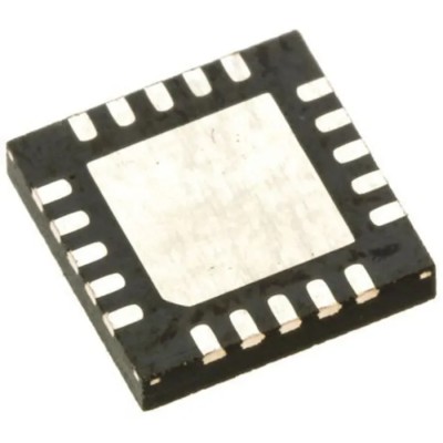
Comes in a small footprint 8-pin SOIC package measuring 4.9mm in length and 1mm in height, the Clock Buffer is well suited for densely packed printed circuit boards. Operating over an ambient temperature range of -40°C to 85°C, it meets the demands of industrial and commercial environments.
Powered at 3.3V core voltage with configurable output voltage levels of 3.3V, 2.5V, or 1.8V, it offers compatibility with multiple logic families and power domains. This wide voltage and temperature range enhances its adaptability for diverse applications including communications, computing, and embedded system clock distribution.
Supports differential input types: LVPECL, LVDS, LVHSTL, HCSL, SSTL. Maximum output frequency: 350MHz with low output skew of 15ps. Compact 8-pin SOIC package conserves board space. Wide operating temperature: -40°C to 85°C.
Flexible output voltage options: 3.3V, 2.5V, and 1.8V. Low additive phase jitter ensures high signal integrity. Useful in industrial, communications, computing, and embedded systems. This component is a standard choice for applications requiring precise clock timing and reliable signal distribution from differential sources onto single-ended logic devices.
Explore our range of clock drivers and distribution ICs for related timing and buffering solutions on EnvMart.
Review sent
Your review cannot be sent
Global Payments 140+ Countries

Global Shipping Fedex/UPS/DHL/Aramex/
BlueDart/Delhivery/DP World
24/7 Customer Support Email/Chat/Telephonic Support
Comments (0)
Your review appreciation cannot be sent
Report comment
Report sent
Your report cannot be sent