


Previous
Next
Share
Free Delivery in India | Lowest Global Shipping Charges
24/7 Customer Support

Shop with confidence knowing that our 24/7 Customer Support is always available to assist with any inquiries

24/7 Customer Support
Save up to 28% with GST Input

Avail maximum benefits from input tax mechanism on all your Business Invoices. Get GST Invoices on your business purchases. And 0% Taxes on all worldwide deliveries

Lowest Price Challenge
# Lowest Price Challenge

If you find this product anywhere at lower cost than us. Call us and we will not only match the price but also give a complimentary coupon

Lowest Price Challenge
100% Original Products

Shop with assurance, as each product we offer is 100% original, ensuring quality and authenticity with every purchase

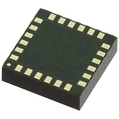
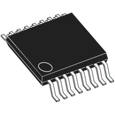
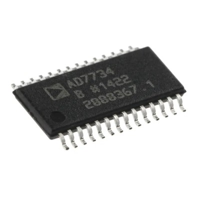
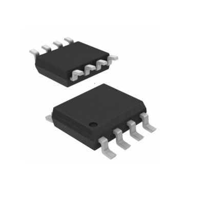
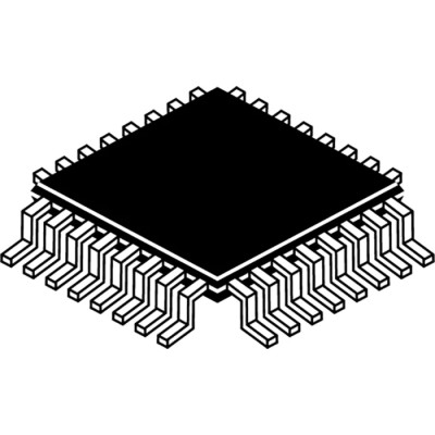
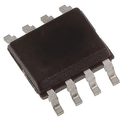
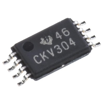
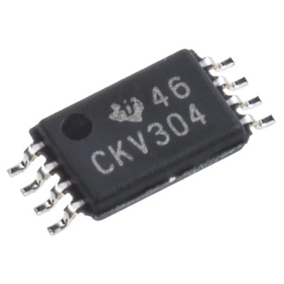
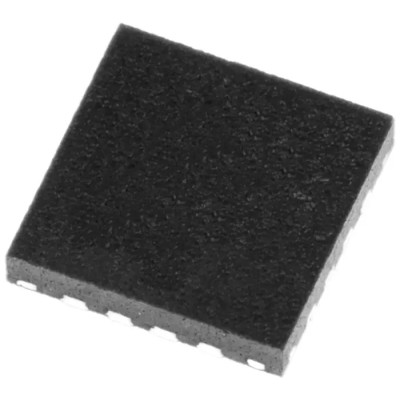
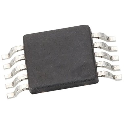
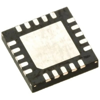
Renesas Electronics PLL Clock Driver, 3.3 V, 166 MHz, 20-Pin QSOP Package 49FCT3805AQG

Specifications

Country of Origin India
Brand Renesas Electronics
Height 1.47mm
Length 8.7mm
Model 49FCT3805AQG
Mount Type Surface
Series 49FCT3805A
Maximum Operating Temperature 70°C
Package Type QSOP
Minimum Operating Temperature 0°C
Maximum Output Frequency 166MHz
Pin Count 20
Maximum Supply Voltage 3.3V
Minimum Supply Voltage 3V

Key Features

  • Operates at a minimum supply voltage of 3 V and maximum of 3.3 V.
  • Supports a maximum output frequency of 166 MHz suitable for high-speed applications.
  • Features a 20-pin QSOP surface-mount package for compact mounting.
  • Operating temperature ranges from 0°C to 70°C ensuring device reliability.
  • Equipped with a heartbeat monitor for diagnostics and PLL driving.
  • Constructed using advanced dual metal CMOS technology enabling low capacitance inputs with hysteresis.
  • TTL compatible inputs and outputs, and inputs compatible with 3.3 V and 5 V components.
  • Low duty cycle distortion of less than 1.0 ns and guaranteed low skew under 500 ps maximum.

Product Description

Renesas Electronics 49FCT3805AQG PLL Clock Driver is a high-performance clock distribution integrated circuit designed to operate at 3.3 volts with a maximum output frequency of 166 MHz. Manufactured with advanced dual metal CMOS technology, this device facilitates precise timing signal distribution in electronic systems where signal quality and skew are critical.

The device features a 20-pin QSOP surface mount package with typical dimensions of 8.7 mm in length and 1.47 mm in height, providing a compact footprint ideal for modern PCB designs. It has two separate output banks, each with a 1:5 fanout and independent 3-state output enable control, which allows flexible clock signal management. The built-in heartbeat monitor output supports diagnostics and phase-locked loop (PLL) driving requirements.

The device supports a supply voltage range between 3 V minimum and 3.3 V maximum, ensuring compatibility with various system voltages. It operates reliably within the temperature range of 0°C to 70°C and does not comply with any automotive-specific standards, making it suitable primarily for commercial and industrial electronics applications.

Key electrical features include low capacitance inputs with hysteresis, TTL compatible inputs and outputs, and the ability to be driven from either 3.3 V or 5 V logic levels. The clock driver ensures very low duty cycle distortion of less than 1.0 nanosecond and maximum skew below 500 picoseconds, essential for minimizing timing errors in sensitive circuits.

Operates on 3.3 V ± 0.3 V supply voltage. Offers two independent output banks with 1:5 fanout each and 3-state output capability. Includes a heartbeat monitor identical to output pins for system diagnostics. Built with 0.5 micron CMOS technology ensuring low power consumption.

Package options include SSOP, SOIC, and QSOP for versatile mounting solutions.

This PLL clock driver is widely used in industrial, telecommunications, computing, and measurement equipment where precise clock timing and distribution to multiple loads are crucial. Its low power operation and high signal integrity make it suitable for embedded systems and high-speed digital applications.

Explore additional electronic components and semiconductor solutions at EnvMart to complement your design and development requirements.

Explore more products in our Clock Drivers & Distribution category.

Renesas Electronics PLL Clock Driver, 3.3 V, 166 MHz, 20-Pin QSOP Package 49FCT3805AQG
Looking to purchase in bulk?
  • Purchase item in bulk quantity
  • Get best price for your business

Comments (0)

No customer reviews for the moment.

Frequently Asked Questions

The maximum output frequency of this model is 166 MHz, making it suitable for high-speed applications.

It operates within a supply voltage range of 3 V minimum to 3.3 V maximum.

The typical dimensions of the package are 8.7 mm in length and 1.47 mm in height.

This model operates reliably within a temperature range of 0°C to 70°C.

It features two independent output banks, each with a 1:5 fanout and independent 3-state output enable control.

It has TTL compatible inputs and outputs, and can be driven from either 3.3 V or 5 V logic levels.

Yes, it is equipped with a heartbeat monitor output that supports diagnostics and PLL driving requirements.

It is constructed using advanced dual metal CMOS technology, which enables low capacitance inputs with hysteresis.

The clock driver ensures a low duty cycle distortion of less than 1.0 nanosecond.

It is widely used in industrial, telecommunications, computing, and measurement equipment where precise clock timing and distribution are crucial.

The country of origin for the 49FCT3805AQG is India.

Related Products

Other Products from this brand

$23.16
$20.22 Save 12.7%
Tax included
Quantity
Delivery Time Delivered within 0-3 days
  • Global Payments 140+ CountriesGlobal Payments 140+ Countries
  • Global Shipping Fedex/UPS/DHL/Aramex/
BlueDart/Delhivery/DP WorldGlobal Shipping Fedex/UPS/DHL/Aramex/ BlueDart/Delhivery/DP World
  • 24/7 Customer Support Email/Chat/Telephonic Support24/7 Customer Support Email/Chat/Telephonic Support
$23.16
$20.22
Tax included